Introduction
Printed Circuit Board (PCB) design is a critical process in electronics development, requiring precision to ensure functionality and reliability. Among the various specifications, 1 oz copper remains a standard choice for many applications due to its balance of cost and performance. However, common PCB errors often arise when working with this copper thickness, leading to performance issues or manufacturing challenges. For electrical engineers, understanding these PCB design mistakes and mastering PCB troubleshooting techniques are essential skills. This article explores frequent pitfalls associated with 1 oz copper PCB errors, offering practical solutions and best practices for avoiding PCB design problems. By following industry standards and proven methods, engineers can enhance design quality and minimize costly revisions. Let’s delve into the specifics of 1 oz copper and the errors to watch for.
What Is 1 oz Copper in PCB Design and Why It Matters
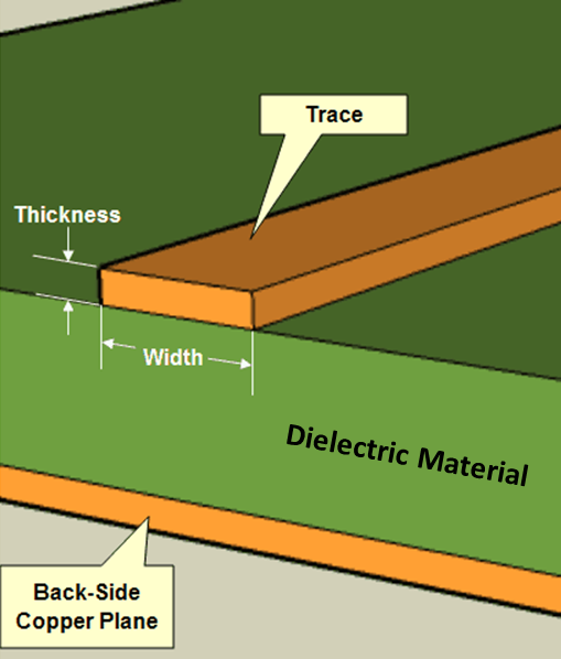
In PCB design, copper thickness is measured in ounces per square foot, indicating the weight of copper spread over a defined area. A 1 oz copper layer translates to approximately 1.4 mils or 35 micrometers in thickness. This standard is widely used in consumer electronics, prototyping, and low to medium power applications due to its affordability and ease of manufacturing. Its relevance lies in providing sufficient current carrying capacity for many circuits while keeping production costs low.
However, 1 oz copper has limitations in high current or high frequency designs where thermal management and signal integrity become critical. Misjudging its capabilities often leads to common PCB errors, such as overheating or inadequate trace widths. For electrical engineers, selecting 1 oz copper requires a clear understanding of the application’s electrical and thermal demands to prevent PCB design mistakes. Proper design with this thickness ensures reliability without unnecessary material expenses.
Technical Principles Behind 1 oz Copper PCB Errors
Understanding the root causes of 1 oz copper PCB errors begins with recognizing the material’s electrical and thermal properties. The current carrying capacity of a 1 oz copper trace depends on its width and the acceptable temperature rise. Narrow traces can overheat under high current, leading to delamination or failure as per guidelines in IPC-2221B, which provides standards for trace width calculations based on current and temperature constraints.
Signal integrity is another concern, especially in high speed designs. Thin copper layers like 1 oz may contribute to higher resistance and impedance mismatches if not carefully planned. This can result in signal degradation or crosstalk. Additionally, thermal dissipation is limited with 1 oz copper, making it prone to hot spots in densely packed boards or power heavy applications.
Manufacturing constraints also play a role in PCB design mistakes. Etching precision for 1 oz copper must be controlled to avoid over etching, which reduces trace width and impacts current capacity. As outlined in IPC-A-600K, acceptable tolerances for copper thickness and trace dimensions must be adhered to during fabrication to prevent defects. These technical factors highlight why avoiding PCB design problems requires meticulous attention to detail.
Common PCB Design Mistakes with 1 oz Copper
Several recurring issues plague designs using 1 oz copper, often due to oversight or miscalculation. Below are the most frequent PCB design mistakes electrical engineers encounter.
Inadequate Trace Width for Current Load
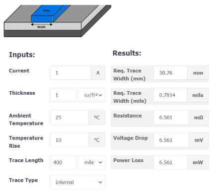
One of the primary errors is underestimating the current a trace must carry. Narrow traces with 1 oz copper cannot handle high currents without excessive heat buildup. This violates principles in IPC-2221B, which specifies minimum trace widths for given current levels to ensure safety and performance.
Poor Thermal Management Planning
Designs often neglect heat dissipation, assuming 1 oz copper can manage thermal loads. Without proper spacing or vias for heat transfer, components may overheat, leading to failure. This is a critical oversight in power electronics where heat accumulation is significant.
Ignoring Signal Integrity in High Speed Circuits
For high frequency signals, 1 oz copper may not provide the necessary impedance control if trace geometry and layer stackup are not optimized. This results in signal loss or interference, a common issue in digital circuits requiring precise timing.
Insufficient Clearance and Spacing
Manufacturing limitations with 1 oz copper require specific clearance between traces to avoid short circuits during etching. Failing to meet minimum spacing as per IPC-6012E standards can lead to defects or reliability issues during operation.
Overlooking Manufacturing Tolerances
Designers sometimes ignore fabrication tolerances, assuming ideal conditions. Over etching or under etching of 1 oz copper traces can alter dimensions, affecting performance. Adhering to tolerances specified in IPC-A-600K is vital to prevent such discrepancies.
Practical Solutions for Avoiding PCB Design Problems
Addressing these common PCB errors involves a combination of design foresight and adherence to industry standards. Below are actionable strategies for PCB troubleshooting and error prevention with 1 oz copper.
Calculate Trace Widths Accurately
Use established guidelines from IPC-2221B to determine appropriate trace widths based on current requirements and temperature rise limits. Software tools that incorporate these standards can assist in automating calculations, ensuring traces are neither too narrow nor unnecessarily wide.
Enhance Thermal Management
Incorporate thermal vias and wider copper areas to dissipate heat effectively. Spacing components to avoid clustering heat sources also helps. For power intensive designs, consider if 1 oz copper is sufficient or if a thicker layer is warranted based on thermal analysis.
Optimize for Signal Integrity
For high speed applications, maintain consistent impedance by controlling trace geometry and layer stackup. Use simulation tools to predict signal behavior and adjust designs to minimize crosstalk or reflections, especially with the limitations of 1 oz copper.
Adhere to Clearance Standards
Ensure designs meet minimum spacing and clearance requirements as per IPC-6012E. This prevents manufacturing defects like shorts or insufficient insulation between conductive paths. Always verify design rules against fabrication capabilities.
Validate Designs with DFM Checks
Perform Design for Manufacturability (DFM) reviews to catch potential issues related to etching tolerances or copper thickness variations. Referencing IPC-A-600K for acceptable criteria ensures the design aligns with manufacturing realities, reducing the risk of 1 oz copper PCB errors.
Troubleshooting 1 oz Copper PCB Errors Post Fabrication
Even with careful planning, issues can emerge after manufacturing. Effective PCB troubleshooting is crucial to identify and resolve problems with 1 oz copper boards. Start by visually inspecting the board for signs of over etching or trace damage, comparing against acceptability criteria in IPC-A-600K. Use a multimeter to check for continuity issues or shorts between traces, focusing on areas with tight spacing.
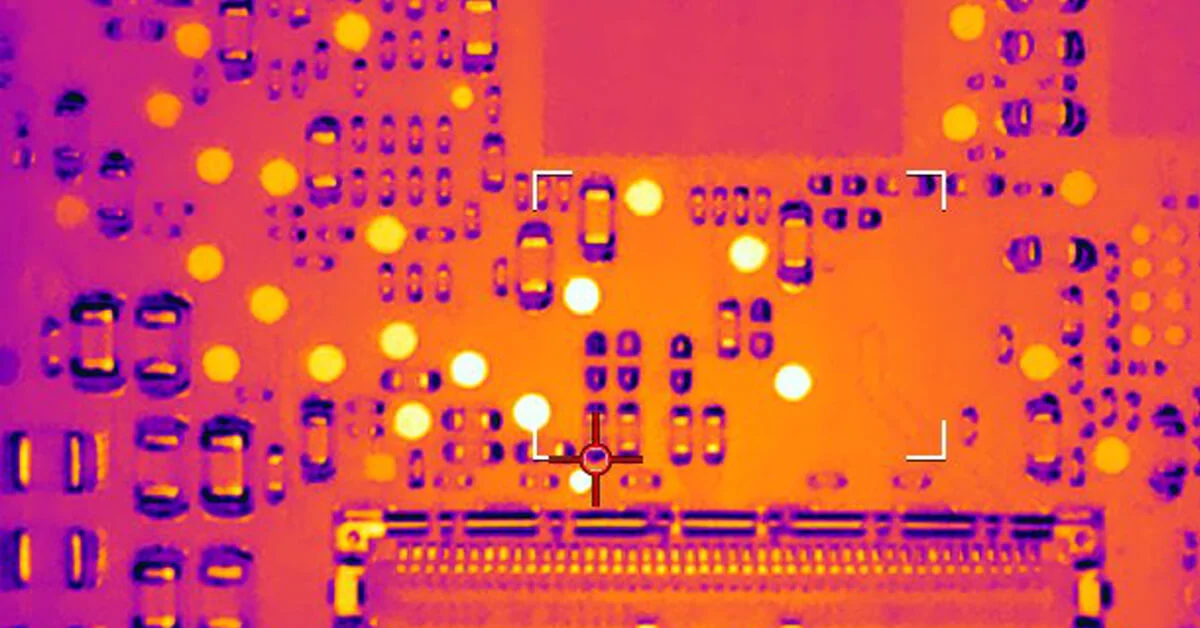
For thermal problems, employ infrared imaging to locate hot spots, indicating inadequate copper area or poor heat dissipation. If signal integrity issues are suspected, oscilloscopes can help analyze waveform distortions or timing errors, pointing to impedance mismatches. Document findings and correlate them with design parameters to pinpoint root causes. Adjustments might include redesigning specific sections or adding heat sinks for thermal relief.
Collaboration with fabrication teams ensures issues like etching inconsistencies are addressed in future iterations. Keeping detailed records of troubleshooting outcomes aids in refining design practices, ultimately avoiding PCB design problems in subsequent projects.
Best Practices for Long Term Success
Beyond immediate fixes, adopting consistent habits prevents recurring 1 oz copper PCB errors. Always start with a thorough requirements analysis, defining current, thermal, and signal needs before selecting copper thickness. Regularly update design rules to align with the latest revisions of standards like IPC-6012E and IPC-2221B, ensuring compliance with evolving industry norms.
Simulate designs under worst case scenarios to anticipate failure points. This proactive approach identifies weaknesses early, saving time and resources. Maintain open communication with manufacturing teams to understand their capabilities and limitations with 1 oz copper processing. Finally, invest in continuous learning about PCB design mistakes through technical resources and industry publications to stay informed on emerging challenges and solutions.
Conclusion
Designing quick turn PCB boards with 1 oz copper offers a cost effective solution for many applications, but it demands careful attention to avoid common PCB errors. Electrical engineers must prioritize accurate trace sizing, thermal management, and signal integrity while adhering to manufacturing constraints. By following standards such as IPC-2221B, IPC-6012E, and IPC-A-600K, designers can mitigate risks associated with 1 oz copper PCB errors. Implementing the best practices and PCB troubleshooting techniques outlined ensures reliable performance and reduces costly redesigns. With a structured approach, avoiding PCB design problems becomes an achievable goal, enhancing overall project success.
FAQs
Q1: What are the most frequent PCB design mistakes with 1 oz copper?
A1: The most frequent PCB design mistakes include inadequate trace widths for current loads, poor thermal management, and ignoring signal integrity needs. Narrow traces overheat, while insufficient heat dissipation causes component failure. High speed circuits may suffer from impedance issues. Adhering to standards like IPC-2221B for trace sizing helps prevent these errors during design.
Q2: How can engineers avoid PCB design problems with 1 oz copper thickness?
A2: Engineers can avoid PCB design problems by calculating trace widths per current requirements, using thermal vias for heat dissipation, and ensuring proper spacing as per IPC-6012E. Simulation tools help predict performance issues. Conducting DFM checks before fabrication also aligns designs with manufacturing tolerances, reducing the risk of defects.
Q3: What steps are involved in PCB troubleshooting for 1 oz copper errors?
A3: PCB troubleshooting starts with visual inspection for trace damage or etching issues, guided by IPC-A-600K standards. Use a multimeter for continuity checks and infrared imaging for thermal hot spots. Oscilloscopes identify signal integrity problems. Documenting issues and collaborating with fabrication teams ensures corrective actions for future designs.
Q4: Why does 1 oz copper lead to common PCB errors in high current designs?
A4: In high current designs, 1 oz copper often leads to common PCB errors due to its limited current carrying capacity. Narrow traces generate excessive heat, risking failure if not sized per IPC-2221B guidelines. Thermal dissipation is also constrained, making it unsuitable without additional cooling strategies or wider copper areas.
References
IPC-2221B — Generic Standard on Printed Board Design. IPC, 2012.
IPC-6012E — Qualification and Performance Specification for Rigid Printed Boards. IPC, 2020.
IPC-A-600K — Acceptability of Printed Boards. IPC, 2020.