Introduction
Copper foil thickness plays a critical role in PCB performance, directly influencing current handling, thermal dissipation, and signal integrity. Electrical engineers often face the challenge of selecting the right thickness early in the design process to balance functionality, manufacturability, and cost. Choosing incorrectly can lead to overheating, excessive trace widths, or unreliable operation under load. This article outlines a structured approach to calculating the ideal copper foil thickness using established engineering principles. By leveraging PCB design tools like PCB trace width calculators and current carrying capacity calculators, designers can optimize their layouts efficiently. Understanding these calculations ensures compliance with reliability standards and enhances overall project success.
What Is Copper Foil Thickness and Why Does It Matter?
Copper foil thickness refers to the weight of copper per square foot, typically measured in ounces per square foot (oz/ft2), which correlates to its physical thickness in microns or mils. Common weights include values around 0.5 oz/ft2, 1 oz/ft2, and 2 oz/ft2, each offering different trade-offs in electrical and mechanical properties. Thicker foils provide greater cross-sectional area for current flow, reducing resistance and allowing narrower traces for the same amperage. This matters in high-power applications where space is limited, as it prevents excessive heating that could degrade components or the board itself.
In PCB design, inadequate thickness leads to voltage drops and thermal hotspots, compromising system reliability. Conversely, overly thick foils increase material costs and complicate fine-line etching during fabrication. Factors like layer count, operating environment, and frequency also influence the choice, making precise calculation essential. Engineers rely on copper thickness calculators to evaluate these variables systematically, ensuring the design meets performance goals without unnecessary over-specification.
Technical Principles Behind Copper Foil Thickness Selection
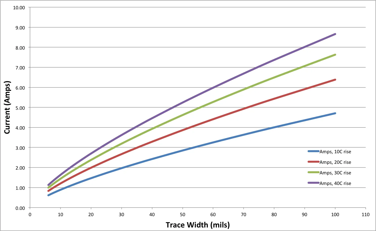
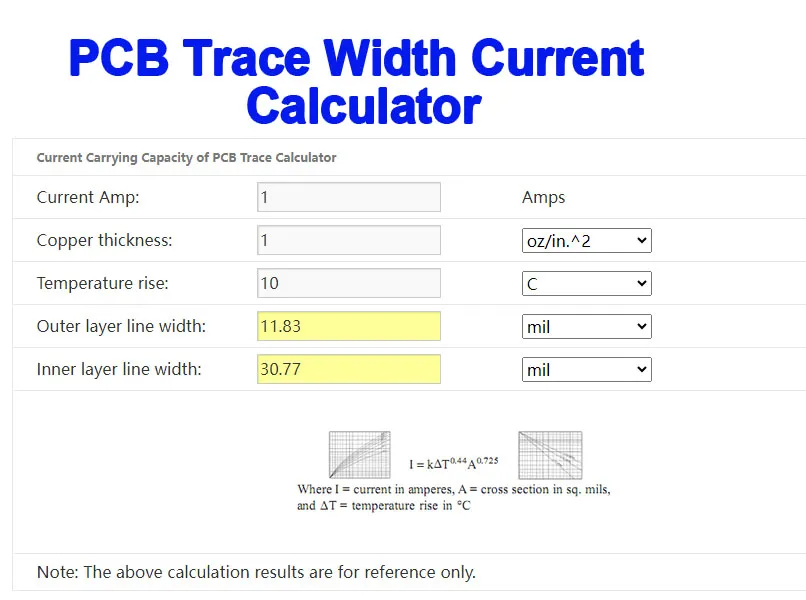
The primary principle governing copper thickness is current carrying capacity, determined by the trace's cross-sectional area and allowable temperature rise. Resistance in a trace follows Ohm's law, where R = ρL/A, with ρ as copper resistivity, L as length, and A as cross-sectional area. Thicker copper increases A, lowering resistance and I2R losses, which manifest as heat. Standards like IPC-2152 provide charts correlating current, thickness, trace width, and temperature rise for both external and internal layers, accounting for board thickness and copper coverage.
Heat dissipation depends on convection, conduction through the board, and radiation, with external traces cooling more effectively than internal ones due to air exposure. IPC-2221 offered earlier conservative guidelines, but IPC-2152 refined these with empirical data from varied test vehicles, including different board configurations. This evolution allows more accurate predictions, especially for high-density designs. Engineers must consider skin effect at high frequencies, where current flows near the surface, favoring thinner foils for better high-speed performance.
Mechanical aspects include foil adhesion to the substrate and etching uniformity, where heavier weights demand adjusted process parameters. Thicker foils enhance rigidity in rigid-flex boards but raise warpage risks during lamination. Signal integrity requires controlled impedance, often necessitating consistent thickness across layers. These principles underscore the need for integrated analysis using PCB design tools.
Factors Influencing the Ideal Copper Thickness
Several design constraints dictate copper thickness. High-current power rails, such as those in motor drives or power supplies, benefit from 2 oz/ft2 or heavier to minimize trace widths and voltage drops. In contrast, high-frequency RF circuits prefer 0.5 oz/ft2 for lower inductance and better etching resolution. Thermal management is key; environments with poor airflow or high ambient temperatures require thicker copper to limit delta-T to safe levels, typically under 20°C for reliability.
Board stackup plays a role, as internal layers have reduced cooling, often needing 50% wider traces than external for equivalent capacity. Cost escalates with thickness due to more copper and extended plating times, so optimization avoids excess. Manufacturability limits fine features; traces below 4 mils become challenging with heavy copper. Space availability on the board often drives the decision, where a copper thickness calculator reveals if upgrading weight allows routing within constraints.
Regulatory and reliability standards further guide selection. Compliance with IPC guidelines ensures the board withstands expected loads without delamination or electromigration. Future-proofing for redesigns favors versatile thicknesses like 1 oz/ft2.
Step-by-Step Guide to Calculating Ideal Copper Foil Thickness
Start by identifying the maximum steady-state and peak currents for each net, consulting datasheets and simulations for accuracy. Define acceptable temperature rise based on component ratings and ambient conditions, often 10-30°C. Select candidate thicknesses from standard options, inputting them into a current carrying capacity calculator alongside trace length and layer type.
For each thickness, compute required trace width using IPC-2152-based PCB trace width calculators. Compare widths against routing space; if too wide, increment thickness and recalculate. Verify voltage drop: ΔV = I * R, where R derives from resistivity and dimensions, ensuring it stays below 5% of supply. Iterate until the thinnest viable thickness emerges, balancing all factors.
Incorporate via and plane contributions for power distribution. Simulate thermal profiles if possible, adjusting for hotspots. Document assumptions for fabrication quotes, specifying finished copper weight post-etching.
- 0.5 oz/ft2 — Approximately 18 μm — High-density, high-speed
- 1 oz/ft2 — Approximately 35 μm — General-purpose
- 2 oz/ft2 — Approximately 70 μm — High-current
- 3 oz/ft2 — Approximately 105 μm — Power-heavy
Validate with online PCB calculators, which implement IPC equations for quick iterations. Prototype testing confirms predictions, measuring actual temps under load.
Practical Case Study: High-Current Automotive Controller
Consider a multilayer PCB for an automotive controller handling 15A peak on power traces with tight routing space. Initial 1 oz/ft2 yields 8 mm external trace widths per IPC-2152 for 20°C rise, exceeding layer constraints. Switching to 2 oz/ft2 reduces this to 4 mm, fitting the layout while maintaining low resistance.
Internal ground planes at 1 oz/ft2 suffice for return paths, but power layers upgrade for symmetry. Thermal vias enhance heat sinking, dropping effective rise further. This adjustment cut board area by 15%, lowered costs versus redesign, and met reliability specs. Such cases highlight how copper thickness calculators streamline decisions.
Advanced Considerations for Optimized Designs
For mixed-signal boards, balance thickness across layers to control impedance. Differential pairs may need thinner foils for 50-ohm matching. In high-reliability sectors, factor aging; copper migrates under current, thickening narrowing over time. Use J-STD guidelines for assembly compatibility.
Multilayer thermal coupling affects capacity; dense planes boost it. Edge effects near board edges alter dissipation. Software PCB design tools integrate these for holistic optimization.
Conclusion
Calculating ideal copper foil thickness demands a methodical evaluation of current, thermal, and spatial factors using IPC-2152 principles. Start with standard weights, leverage current carrying capacity calculators and PCB trace width calculators for precision, and iterate for the optimal balance. This approach minimizes risks, controls costs, and ensures robust performance. Electrical engineers who master these calculations deliver superior designs ready for production.
FAQs
Q1: How does a PCB trace width calculator help with copper thickness selection?
A1: A PCB trace width calculator uses IPC-2152 data to compute required widths for given currents, thicknesses, and temperature rises. Input your max current and space limits, test thicknesses from 0.5 to 2 oz/ft2, and select the one yielding feasible widths. This tool prevents undersizing, avoiding failures, and optimizes layouts efficiently. Always verify external vs. internal layer differences for accuracy.
Q2: What role does a copper thickness calculator play in high-power PCB projects?
A2: Copper thickness calculators determine the minimum weight for safe current handling under thermal constraints. Enter current, allowable rise, and trace constraints to find if 1 oz/ft2 suffices or if heavier is needed. They incorporate standards like IPC-2152 for reliable predictions, aiding power electronics designs. This ensures low resistance without excessive widths or costs.
Q3: Can online PCB calculators replace manual IPC-2152 chart analysis?
A3: Online PCB calculators automate IPC-2152 charts, handling variables like layer type and board thickness for current carrying capacity. They provide instant iterations, surpassing manual graphing speed while maintaining accuracy. Use them for initial sizing, then validate with simulations. Ideal for complex stackups where charts alone fall short.
Q4: When should electrical engineers upgrade to heavier copper in PCB design tools?
A4: Upgrade when standard 1 oz/ft2 traces exceed space or cause high drops, as shown in PCB design tools. High-current nets over 10A or poor cooling environments demand 2 oz/ft2 for narrower paths per IPC-2152. Balance with etch limits and costs for optimal results.
References
IPC-2152B — Standard for Determining Current-Carrying Capacity in Printed Board Design. IPC, 2019
IPC-2221B — Generic Standard on Printed Board Design. IPC, 2012
IPC-6012E — Qualification and Performance Specification for Rigid Printed Boards. IPC, 2017