Introduction
Mixed signal PCB design combines analog and digital circuitry on a single board, presenting unique challenges for electrical engineers. These designs are critical in applications ranging from consumer electronics to automotive system design, where precision and reliability are paramount. The primary obstacles include managing noise interference, maintaining signal integrity, and ensuring compatibility between analog and digital components. Overcoming these signal PCB challenges requires a deep understanding of both circuit behaviors and layout techniques. This article explores the core issues in mixed signal PCB design, focusing on noise interference solutions and considerations for automotive applications. By following established industry practices and standards, engineers can achieve robust designs that meet stringent performance requirements. Let's delve into the technical principles and practical strategies to address these challenges effectively.
What Is Mixed Signal PCB Design and Why It Matters
Mixed signal PCB design refers to the integration of analog and digital circuits on the same printed circuit board. Analog components handle continuous signals, such as voltages or currents, while digital components process discrete binary data. This combination is essential in modern electronics, where devices often require both types of processing. For instance, in automotive system design, mixed signal PCBs are used in sensors, control units, and infotainment systems, converting real-world inputs into digital data for processing.
The importance of mixed signal design lies in its ability to enable compact, efficient, and multifunctional systems. However, the coexistence of analog and digital signals introduces significant signal PCB challenges. Noise interference from digital switching can disrupt sensitive analog signals, leading to performance degradation. Addressing these issues is critical to ensure reliability, especially in demanding environments like automotive applications where safety and precision are non-negotiable.
Technical Principles Behind Mixed Signal PCB Challenges
Understanding the root causes of challenges in mixed signal PCB design is the first step toward effective solutions. The primary issue stems from the fundamental differences between analog and digital signals. Digital circuits operate with rapid switching, generating high-frequency noise that can couple into analog sections through shared power supplies, ground planes, or electromagnetic fields. This noise interference can distort analog signals, leading to inaccurate readings or system failures.
Another key challenge is maintaining signal integrity across the board. Analog signals are sensitive to impedance mismatches, crosstalk, and parasitic effects, while digital signals require controlled impedance for timing accuracy. In automotive system design, these issues are compounded by harsh operating conditions, including temperature fluctuations, vibrations, and electromagnetic interference from nearby systems.
Power supply noise is also a critical concern. Digital circuits often draw current in sharp bursts, causing voltage ripples that affect analog components. Without proper isolation or filtering, these disturbances can degrade performance. Additionally, layout constraints, such as limited board space, often force engineers to place sensitive components closer than ideal, increasing the risk of interference.
Key Challenges in Mixed Signal PCB Design
Noise Interference
Noise interference remains the most significant signal PCB challenge in mixed signal designs. Digital circuits produce high-frequency harmonics during switching, which can induce unwanted currents or voltages in analog traces through capacitive or inductive coupling. This interference can manifest as jitter, offset errors, or reduced signal-to-noise ratio in analog circuits.
Grounding Conflicts
Improper grounding is a common source of noise in mixed signal PCBs. Using a single ground plane for both analog and digital sections can allow digital noise to propagate into analog areas. This is particularly problematic in automotive system design, where external electromagnetic fields can exacerbate grounding issues.
Power Supply Coupling
Shared power supplies between analog and digital domains often lead to noise coupling. Voltage fluctuations caused by digital load changes can affect analog components, especially in high-precision applications. Without adequate decoupling or filtering, these fluctuations compromise system stability.
Component Placement and Routing
Placing analog and digital components in close proximity increases the likelihood of interference. Routing high-speed digital traces near sensitive analog lines can introduce crosstalk. Limited board space often makes ideal separation difficult, requiring careful planning to minimize risks.
Practical Solutions for Mixed Signal PCB Design Challenges
Addressing the challenges in mixed signal PCB design requires a combination of strategic planning, adherence to best practices, and compliance with industry standards. Below are actionable noise interference solutions and design guidelines tailored for electrical engineers.
Ground Plane Separation
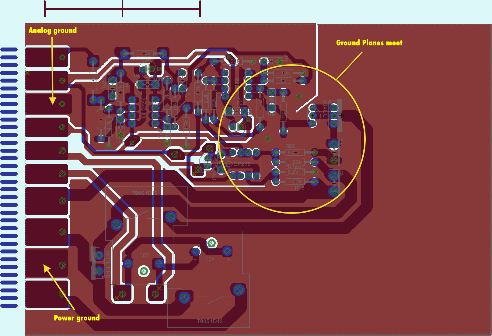
One effective approach to mitigate noise interference is to separate analog and digital ground planes. This involves creating distinct ground regions for each domain, connected at a single point to avoid ground loops. This technique, often referred to as a star grounding scheme, minimizes the transfer of digital noise into analog sections. According to guidelines in IPC-2221B, Generic Standard on Printed Board Design, careful ground plane partitioning is essential for maintaining signal integrity in mixed signal systems.
Power Supply Isolation
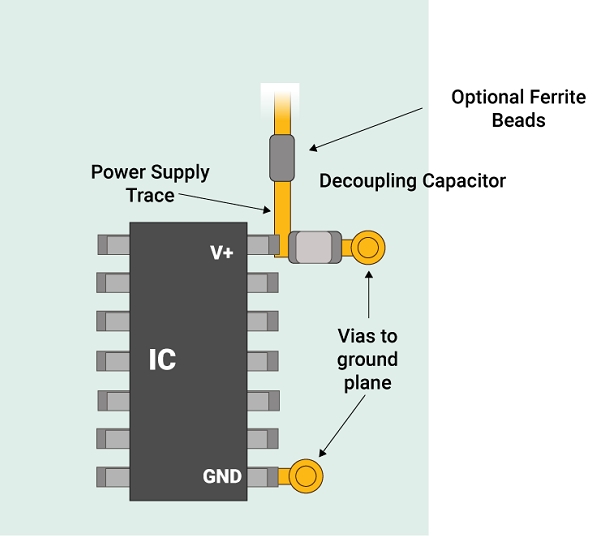
Isolating power supplies for analog and digital circuits is another critical noise interference solution. Using separate voltage regulators for each domain prevents digital switching noise from affecting analog components. Additionally, placing decoupling capacitors close to power pins of digital components helps filter out high-frequency noise. Ferrite beads can also be used in series with power lines to block high-frequency disturbances while allowing DC current to pass.
Related Reading: Power Plane Decoupling: A Comprehensive Guide to PCB Stability
Strategic Component Placement
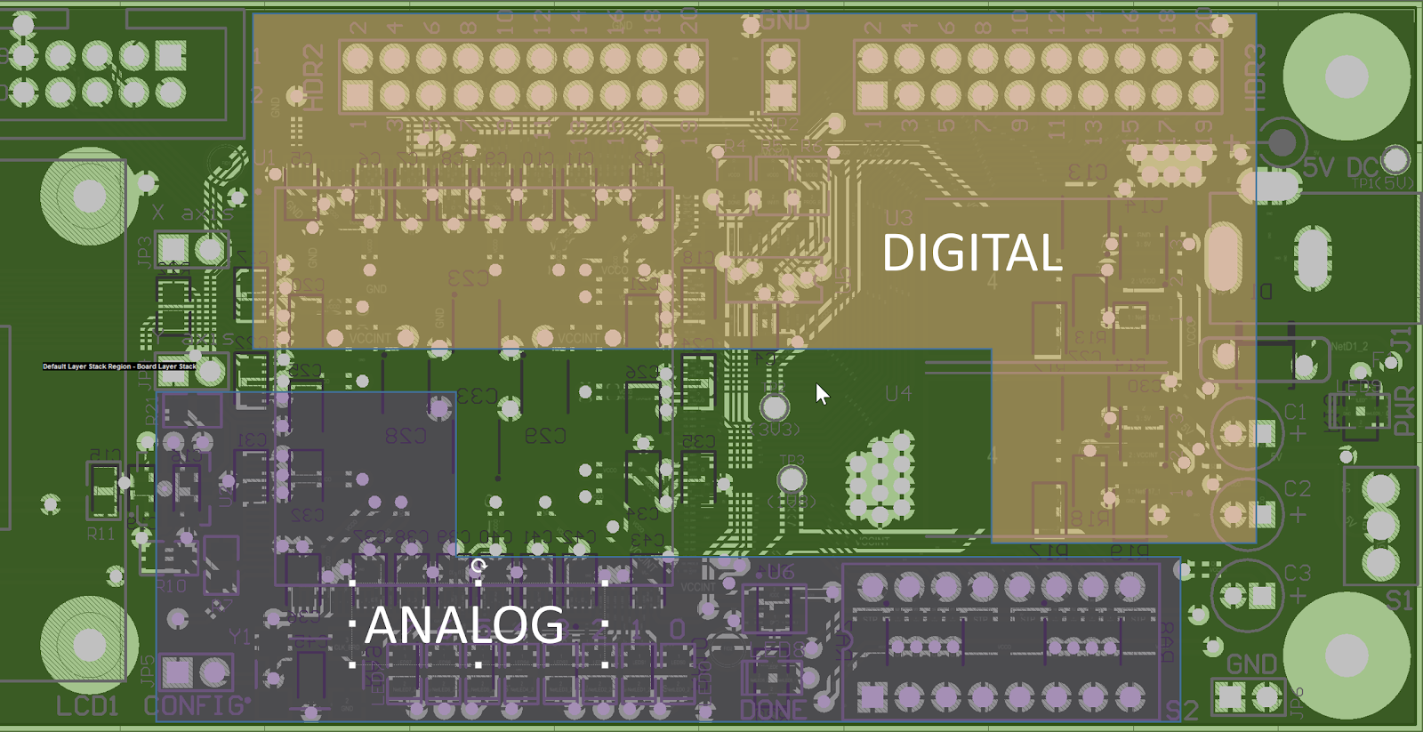
Proper placement of components is vital in mixed signal PCB design. Analog components, such as amplifiers and sensors, should be positioned away from noisy digital circuits like microcontrollers or switching regulators. Grouping similar functions together and maintaining physical separation reduces the risk of interference. For automotive system design, where board space may be constrained, shielding sensitive analog areas with ground planes or guard traces can provide additional protection.
Controlled Routing Practices
Routing high-speed digital traces away from analog signals is essential to avoid crosstalk. When separation is not feasible, routing digital traces perpendicular to analog traces minimizes coupling. Using shorter traces for high-frequency signals reduces parasitic effects. Adhering to standards like IPC-2251, Design Guide for High-Speed Controlled Impedance Circuit Boards, ensures that impedance is managed effectively to maintain signal integrity.
Filtering and Shielding
Incorporating low-pass filters in analog signal paths can attenuate high-frequency noise originating from digital circuits. Shielding techniques, such as enclosing sensitive areas with grounded metal layers, help block external electromagnetic interference, a critical consideration in automotive system design. Compliance with IEC 61000-4-3, which addresses electromagnetic compatibility testing, can guide engineers in implementing effective shielding solutions.
Simulation and Testing
Before finalizing a design, simulation tools can predict potential noise interference issues and validate layout choices. Testing prototypes under real-world conditions, especially for automotive applications, ensures that the PCB performs reliably across temperature ranges and vibration levels. Following testing protocols outlined in ISO 16750-3, Environmental Conditions and Testing for Electrical and Electronic Equipment, helps verify robustness in harsh environments.
Special Considerations for Automotive System Design
Automotive system design introduces additional complexities to mixed signal PCB design due to stringent safety and reliability requirements. PCBs in vehicles must withstand extreme temperatures, humidity, and mechanical stress while maintaining performance. Noise interference solutions become even more critical in this context, as electromagnetic interference from engines, motors, or communication systems can disrupt sensitive circuits.
Designing for automotive applications often involves adhering to standards like ISO 26262, Functional Safety of Road Vehicles, which emphasizes risk assessment and mitigation in electronic systems. Mixed signal PCBs in advanced driver assistance systems or electric vehicle battery management must prioritize low noise and high accuracy. Using robust materials and ensuring thermal management through proper heat dissipation techniques are also essential to prevent failures under stress.
Moreover, automotive designs frequently require redundancy and fault tolerance. Engineers must account for potential noise-induced errors by incorporating error-checking mechanisms in digital circuits and high-precision components in analog sections. Rigorous testing, aligned with AEC-Q100 standards for integrated circuits, ensures that designs meet automotive-grade reliability.
Related Reading: Thermal Management for Mixed Signal PCBs: Best practices
Conclusion
Mixed signal PCB design presents significant challenges due to the coexistence of analog and digital signals on a single board. Noise interference, grounding conflicts, and power supply coupling are among the primary signal PCB challenges that engineers must address. By implementing practical noise interference solutions such as ground plane separation, power supply isolation, and strategic component placement, designers can achieve reliable performance. Special attention to automotive system design ensures that PCBs meet the rigorous demands of safety and environmental conditions. Adhering to established industry standards and leveraging simulation tools further enhances design success. With careful planning and execution, electrical engineers can overcome the complexities of mixed signal PCB design and deliver robust, high-performance systems.
FAQs
Q1: What are the main signal PCB challenges in mixed signal design?
A1: In mixed signal PCB design, the primary challenges include noise interference from digital switching affecting analog signals, grounding conflicts, and power supply coupling. These issues can degrade signal integrity and performance. Proper separation of analog and digital domains, along with strategic layout practices, helps mitigate these problems effectively.
Q2: How can noise interference solutions improve PCB performance?
A2: Noise interference solutions, such as using separate ground planes and decoupling capacitors, significantly enhance PCB performance. They prevent digital noise from disrupting analog signals, ensuring accuracy and stability. Filtering techniques and shielding also reduce external interference, which is vital for applications requiring high precision like sensors or audio systems.
Q3: Why is automotive system design critical for mixed signal PCBs?
A3: Automotive system design is crucial for mixed signal PCBs due to the harsh operating conditions and safety requirements in vehicles. PCBs must resist temperature extremes, vibrations, and electromagnetic interference while maintaining reliability. Adhering to strict standards ensures that systems like driver assistance or battery management function without failure.
Q4: What standards guide noise management in mixed signal PCB design?
A4: Standards like IPC-2221B for printed board design and IEC 61000-4-3 for electromagnetic compatibility provide guidelines for noise management in mixed signal PCBs. They emphasize grounding, shielding, and layout techniques to minimize interference. Following these ensures designs meet performance and reliability expectations in various applications.
References
IPC-2221B — Generic Standard on Printed Board Design. IPC, 2012.
IPC-2251 — Design Guide for High-Speed Controlled Impedance Circuit Boards. IPC, 2003.
IEC 61000-4-3 — Electromagnetic Compatibility (EMC) - Part 4-3: Testing and Measurement Techniques - Radiated, Radio-Frequency, Electromagnetic Field Immunity Test. IEC, 2020.
ISO 16750-3 — Road Vehicles - Environmental Conditions and Testing for Electrical and Electronic Equipment - Part 3: Mechanical Loads. ISO, 2012.
ISO 26262 — Road Vehicles - Functional Safety. ISO, 2018.