Introduction
Solder mask application is a critical step in PCB fabrication, providing protection to copper traces and influencing the aesthetic appeal of the final board. For electrical engineers, specifying solder mask colors in Gerber files ensures that the design intent translates accurately during the manufacturing process. These files serve as the blueprint for PCB production, communicating every detail from copper layers to mask coverage. Incorrect specifications can lead to manufacturing delays or functional issues. This article explores the importance of solder mask layers, how to define colors within design files, and best practices for seamless integration into the manufacturing workflow. By following standardized methods, engineers can achieve consistency and reliability in their PCB designs.
What Is a Solder Mask and Why It Matters
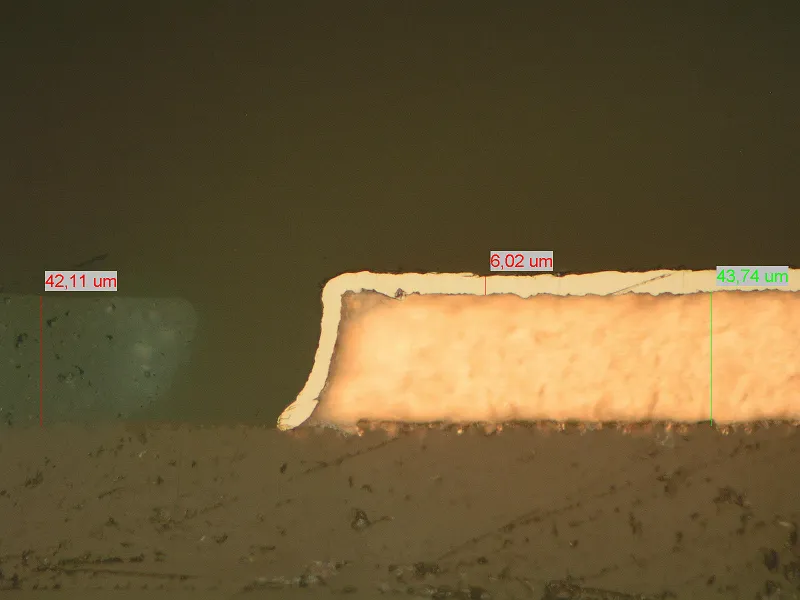
A solder mask is a thin polymer layer applied over the copper traces of a printed circuit board to protect against oxidation and prevent solder bridges during assembly. It acts as an insulating barrier, safeguarding the board from environmental damage and electrical shorts. Beyond functionality, the solder mask contributes to the visual identity of the PCB, with colors often used for branding or differentiation in complex systems.
For electrical engineers, the solder mask layer in Gerber files is vital as it dictates where this protective coating is applied or omitted, such as on pads for soldering. Accurate representation in design files ensures that the manufacturing process aligns with the intended functionality. Errors in this layer can expose copper unnecessarily or cover areas meant for soldering, leading to assembly failures. Thus, precise specification in Gerber files directly impacts the quality and reliability of the final product.
Technical Principles of Solder Mask Layers in Gerber Files
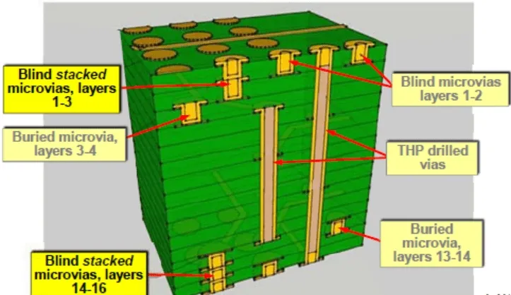
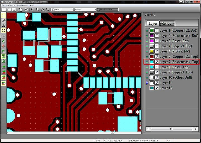
Gerber files are the industry standard format for communicating PCB design data to manufacturers. These vector-based files include separate layers for various elements, such as copper traces, silkscreen, and solder mask. The solder mask layer, often denoted with extensions like GTS for top side and GBS for bottom side per common conventions, defines areas where the mask should be applied or left clear.
Importantly, Gerber files themselves do not inherently carry color information for the solder mask. The color is a manufacturing parameter, not a design file attribute. Instead, the solder mask layer in Gerber files indicates the presence or absence of the mask through positive or negative imaging, depending on the software and manufacturer requirements. A positive image means the drawn areas receive the mask, while a negative image indicates openings where the mask is absent.
Engineers must ensure that the solder mask layer aligns with the copper layer to avoid mismatches during PCB fabrication. Standards like IPC-6012E provide guidelines for acceptable tolerances and coverage to prevent issues such as mask encroachment on pads. Following such standards ensures that the design files are interpreted correctly during the manufacturing process, minimizing errors.
How to Specify Solder Mask Colors for Manufacturing
While Gerber files define the solder mask coverage, the color specification typically occurs outside these design files. Electrical engineers must communicate color preferences separately through documentation or direct communication with the manufacturer. Below are actionable steps to ensure accurate color specification during PCB fabrication.
Step 1: Define Solder Mask Color in Design Notes
Include a detailed fabrication note or drawing alongside the Gerber files. Specify the desired solder mask color, such as green, blue, red, black, or white, in a readme file or technical drawing. This document should accompany the design files during submission to the manufacturer. Clarity in this step prevents misinterpretation, as Gerber files lack color data.
Step 2: Confirm Manufacturer Capabilities
Not all manufacturers offer a wide range of solder mask colors. Standard options often include green due to its historical prevalence and cost-effectiveness. Non-standard colors like purple or yellow may incur additional costs or lead times. Engineers should verify available options and associated constraints before finalizing the design intent.
Step 3: Use Layer Naming Conventions
Ensure that solder mask layers in Gerber files follow standard naming conventions, such as GTS for top solder mask and GBS for bottom. Consistent naming helps manufacturers identify the correct layers during the manufacturing process. Incorrect or ambiguous naming can lead to processing errors, even if color is specified elsewhere.
Step 4: Validate with Design Rule Checks
Before exporting Gerber files, perform design rule checks using PCB design software to confirm that solder mask openings align with solderable areas. Adhering to guidelines in standards like IPC-A-600K ensures that the mask does not interfere with assembly. This step reduces the risk of costly revisions after submission.
Step 5: Communicate During Quotation
When requesting a quote for PCB fabrication, explicitly state the solder mask color requirement. Some manufacturers may assume a default color if not specified. Including this detail early in the communication streamlines the manufacturing process and avoids unexpected outcomes.
Best Practices for Engineers in Solder Mask Specification
To achieve optimal results in PCB fabrication, electrical engineers should adopt the following best practices when preparing design files and specifying solder mask colors.
- Always include a fabrication drawing or note with explicit color instructions to supplement Gerber files.
- Cross-verify solder mask layers against copper layers to ensure alignment and avoid coverage errors.
- Reference industry standards like IPC-6012E for acceptable mask tolerances and application criteria.
- Maintain open communication with the manufacturer to confirm color availability and process compatibility.
- Archive all design files and notes for traceability in case of discrepancies during manufacturing.
Following these practices minimizes errors and ensures that the solder mask application meets both functional and aesthetic requirements.
Common Challenges and Troubleshooting Tips
Specifying solder mask colors and preparing Gerber files can present challenges for engineers, especially when transitioning designs into the manufacturing process. One frequent issue is the assumption that color data is embedded in design files. As clarified earlier, Gerber files only define mask presence, not color. To address this, always provide a separate specification document.
Another challenge arises from mismatched layer definitions, where the solder mask layer does not correspond to the intended areas. This can result in exposed copper or masked pads, disrupting assembly. Engineers can mitigate this by thoroughly reviewing Gerber files using viewer tools before submission. Adhering to standards like IPC-A-600K for acceptability criteria helps identify potential issues early.
Lastly, color inconsistencies may occur if the manufacturer uses a different shade or material than expected. Requesting a sample or color swatch prior to full production can prevent such discrepancies. Proactive communication and validation are key to resolving these challenges effectively.
Conclusion
Specifying solder mask colors in Gerber files is a nuanced but essential aspect of PCB fabrication for electrical engineers. While the design files themselves define the mask coverage areas, color selection must be communicated through separate documentation or direct interaction with the manufacturer. By adhering to industry standards, maintaining clear communication, and following best practices, engineers can ensure that their design intent translates accurately into the manufacturing process. Proper specification not only enhances the functionality of the PCB by protecting copper traces but also achieves the desired aesthetic outcome. With careful preparation of design files and attention to detail, the risk of errors diminishes, paving the way for reliable and visually consistent printed circuit boards.
FAQs
Q1: How do I include solder mask color in my Gerber file for PCB fabrication?
A1: Gerber files do not contain color data for solder mask layers. Instead, specify the desired color in a separate fabrication note or drawing submitted with your design files. Communicate directly with the manufacturer during the quotation or submission process to confirm the color choice. This ensures clarity and prevents assumptions during the manufacturing process.
Q2: Why is the solder mask layer important in design files for engineers?
A2: The solder mask layer in design files defines where protective coating is applied on a PCB, safeguarding copper traces from damage and preventing solder bridges. For engineers, accurate specification in Gerber files is crucial to ensure proper alignment with solderable areas. Errors can lead to functional issues, making this layer vital for reliable PCB fabrication.
Q3: What standards should I follow for solder mask in PCB manufacturing process?
A3: Engineers should adhere to standards like IPC-6012E for performance specifications and IPC-A-600K for acceptability criteria in PCB fabrication. These guidelines outline tolerances for solder mask application, ensuring coverage does not interfere with assembly. Following such standards minimizes errors and enhances the quality of the final product during manufacturing.
Q4: How can I avoid errors in solder mask layers during PCB design?
A4: To avoid errors, validate solder mask layers against copper layers using design rule checks before exporting Gerber files. Ensure consistent layer naming, such as GTS for top mask, and reference standards like IPC-A-600K for guidance. Additionally, review design files with viewer tools and communicate clearly with the manufacturer to confirm specifications.
References
IPC-6012E — Qualification and Performance Specification for Rigid Printed Boards. IPC, 2020.
IPC-A-600K — Acceptability of Printed Boards. IPC, 2020.