Introduction
In the field of electrical engineering, understanding signals and their applications is fundamental to designing and troubleshooting electronic systems. Signals, whether analog or digital, form the backbone of communication, control, and data processing in printed circuit boards (PCBs) and embedded systems. Analog signals represent real-world phenomena like temperature or sound, while analog-to-digital converters (ADCs) bridge the gap between analog inputs and digital processing. Additionally, concepts like analog functions and grounding practices, including AGND and DGND pins, play critical roles in ensuring signal integrity. This article explores the principles behind analog signals, the functionality of ADCs, the importance of analog functions, and best practices for managing AGND and DGND pins in PCB design. Aimed at electrical engineers, this guide provides clear and actionable insights to enhance system performance.
What Are Analog Signals and Why Do They Matter
Analog signals are continuous electrical representations of physical quantities such as voltage, current, or frequency. Unlike digital signals, which operate in discrete states, analog signals vary smoothly over time, reflecting real-world inputs like audio waves or sensor readings. Their importance in electrical engineering lies in their ability to capture nuanced data from the environment, making them essential for applications like medical devices, industrial automation, and telecommunications.
In PCB design, analog signals require careful handling to avoid noise and distortion. Engineers must consider factors like impedance matching and shielding to preserve signal quality. The relevance of analog signals extends to their interaction with digital systems, where conversion processes become necessary. This is where analog-to-digital converters come into play, transforming continuous signals into discrete data for microcontrollers and processors to interpret.
Technical Principles of Analog Signals and Conversion
Understanding Analog Signals
Analog signals are characterized by their continuous nature, meaning they can take any value within a given range. For instance, a microphone converts sound waves into a varying voltage signal. This signal can fluctuate infinitely between minimum and maximum values, providing a direct representation of the input. However, this continuity makes analog signals susceptible to interference, requiring precise design considerations in PCB layouts to minimize noise.
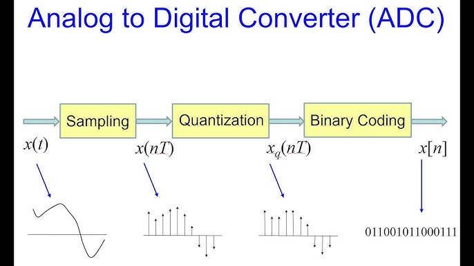
Role of Analog-to-Digital Converters (ADCs)
An analog-to-digital converter is a critical component that transforms analog signals into digital form. ADCs sample the analog input at regular intervals, quantize the amplitude into discrete levels, and encode the data into binary format. This process enables microcontrollers to process real-world inputs. Key parameters of ADCs include resolution, which determines the number of discrete levels, and sampling rate, which affects how accurately the signal is captured. Standards like JEDEC J-STD-020E guide the handling of components like ADCs during assembly to ensure reliability.
Analog Functions in Circuit Design
Analog functions refer to operations performed on analog signals, such as amplification, filtering, or modulation. These functions are vital in conditioning signals before conversion or transmission. For example, amplifiers boost weak signals from sensors, while filters remove unwanted noise frequencies. Implementing analog functions requires a deep understanding of circuit theory and component selection to maintain signal fidelity. Proper PCB design, adhering to standards like IPC-A-600K, ensures that traces and layouts support these functions without introducing errors.
Importance of AGND and DGND Pins in PCB Design
Defining AGND and DGND Pins
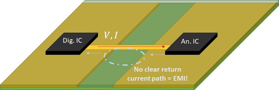
In mixed-signal PCB designs, grounding is a critical aspect that impacts signal integrity. AGND, or analog ground, is dedicated to the analog components of a circuit, providing a clean reference point for sensitive signals. DGND, or digital ground, serves the digital components, which often generate high-frequency noise. Separating AGND and DGND pins helps prevent digital noise from interfering with analog signals, ensuring accurate data acquisition and processing.
Grounding Challenges in Mixed-Signal Systems
One common challenge in PCB design is managing ground loops and noise coupling between analog and digital sections. If AGND and DGND pins are improperly connected, digital switching noise can contaminate analog signals, leading to errors in systems like ADCs. Engineers must design ground planes with care, often using a single ground plane with strategic splits or connecting AGND and DGND at a single point to minimize interference. Guidelines from IPC-6012E provide specifications for PCB fabrication that support effective grounding practices.
Practical Solutions for Signal Integrity and Grounding
Best Practices for Handling Analog Signals
To maintain the integrity of analog signals, engineers should prioritize low-noise design techniques. This includes using proper shielding for traces carrying analog signals and placing sensitive components away from high-speed digital circuits. Additionally, selecting appropriate bypass capacitors near power pins reduces voltage fluctuations. Adhering to standards like IPC-A-600K ensures that PCB manufacturing processes do not introduce defects that could degrade signal quality.
Optimizing ADC Performance
When integrating analog-to-digital converters into a design, engineers must consider several factors to optimize performance. First, ensure that the input signal to the ADC is within its specified range to avoid clipping or distortion. Second, use a stable reference voltage to improve conversion accuracy. Finally, minimize noise at the ADC input by implementing proper filtering and grounding. Following assembly guidelines from JEDEC J-STD-020E helps protect ADC components from damage during soldering.
Strategies for AGND and DGND Pin Management
Effective management of AGND and DGND pins involves creating separate ground planes for analog and digital sections on a PCB. Engineers often connect these planes at a single point, typically near the power supply or ADC, to provide a common reference while reducing noise coupling. Additionally, placing digital components away from analog circuits and routing digital traces perpendicular to analog traces minimizes interference. Fabrication standards like IPC-6012E ensure that the PCB substrate and copper layers support these grounding strategies.
Troubleshooting Common Signal and Grounding Issues
In real-world applications, engineers often encounter issues related to signal distortion or grounding problems. For instance, if an ADC outputs erratic data, the root cause might be noise on the analog input due to poor grounding. To diagnose this, check the connection between AGND and DGND pins and ensure they are tied at a single point. Another common issue is crosstalk between analog and digital traces, which can be mitigated by increasing spacing or using guard traces. Practical experience, combined with adherence to standards like IPC-A-600K, enables engineers to identify and resolve such problems efficiently.
Conclusion
Understanding signals and their applications is essential for electrical engineers working on PCB design and mixed-signal systems. Analog signals serve as the foundation for capturing real-world data, while analog-to-digital converters enable seamless interaction with digital processors. Analog functions like amplification and filtering are crucial for signal conditioning, and proper management of AGND and DGND pins ensures noise-free operation in mixed-signal environments. By following best practices and adhering to recognized industry standards, engineers can design robust systems that deliver reliable performance. This guide provides a comprehensive overview to support such efforts in practical applications.
FAQs
Q1: What are analog signals, and how do they differ from digital signals?
A1: Analog signals are continuous representations of physical quantities, varying smoothly over time, unlike digital signals, which are discrete and binary. In PCB design, analog signals require careful handling to avoid noise interference. They are vital for capturing real-world data from sensors or microphones before conversion to digital form for processing. Understanding their behavior helps engineers design circuits that maintain signal integrity.
Q2: How does an analog-to-digital converter (ADC) function in a circuit?
A2: An analog-to-digital converter transforms continuous analog signals into discrete digital data by sampling, quantizing, and encoding the input. ADCs are essential for interfacing real-world inputs with microcontrollers. Their performance depends on resolution and sampling rate, which determine accuracy. Proper grounding and filtering at the input ensure reliable conversion, making ADCs critical in applications like data acquisition systems.
Q3: Why are AGND and DGND pins important in mixed-signal PCB design?
A3: AGND and DGND pins separate analog and digital grounds to prevent noise from digital circuits from affecting sensitive analog signals. Incorrect grounding can lead to errors in data conversion or signal distortion. Connecting these pins at a single point minimizes interference. This practice is crucial for maintaining signal integrity in mixed-signal systems involving ADCs and analog functions.
Q4: What are common challenges with analog functions in circuit design?
A4: Analog functions like amplification and filtering face challenges such as noise introduction and signal distortion. Poor component placement or inadequate grounding can degrade performance. Engineers must design layouts that isolate analog functions from digital noise sources. Following industry standards for PCB fabrication ensures that these functions operate effectively, supporting accurate signal processing in various applications.
IPC-6012E - Qualification and Performance Specification for Rigid Printed Boards. IPC, 2020.
IPC-A-600K - Acceptability of Printed Boards. IPC, 2020.
JEDEC J-STD-020E - Moisture/Reflow Sensitivity Classification. JEDEC, 2014.