Introduction
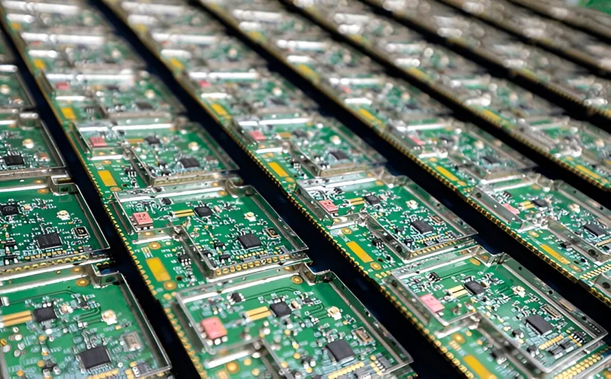
In modern high-speed electronics, printed circuit boards (PCBs) with embedded components represent a significant advancement in miniaturization and performance. These designs integrate passive elements like resistors and capacitors directly into the PCB layers, reducing size and improving electrical efficiency. However, this integration complicates signal transmission, as embedded components can alter local dielectric properties and stackup uniformity. Impedance control PCB techniques become essential to maintain signal integrity across transmission lines. Without precise characteristic impedance management, signals experience reflections, crosstalk, and attenuation, leading to system failures in applications such as telecommunications and computing. This article explores how controlled impedance routing optimizes signal transmission in embedded component PCBs, providing engineers with structured insights for reliable designs.
Electrical engineers designing for frequencies above 1 GHz must prioritize impedance control from the outset. Embedded components impedance variations arise from material interactions and fabrication processes, demanding careful stackup planning. Transmission line PCB structures, whether microstrip or stripline, require consistent impedance to match source and load conditions. By adhering to established principles, designers achieve optimal signal quality and minimize electromagnetic interference.
What Is Impedance Control in PCBs? Why It Matters
Impedance control PCB refers to the process of designing and fabricating traces to maintain a specific characteristic impedance throughout the signal path. Characteristic impedance, denoted as Z0, is the ratio of voltage to current for a propagating wave on an infinite transmission line, typically targeted at 50 ohms for single-ended lines or 100 ohms for differential pairs. In a transmission line PCB, this value depends on the geometry of the conductor and surrounding dielectrics. Deviations cause impedance mismatches, resulting in signal reflections governed by the reflection coefficient formula, Γ = (Z_L - Z0)/(Z_L + Z0).
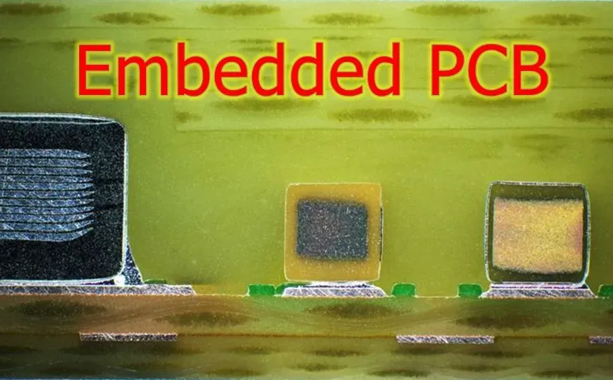
The relevance intensifies in embedded component PCBs, where passives buried within layers disrupt uniform dielectric fields. These disruptions lead to localized impedance discontinuities, exacerbating signal integrity issues like ringing and eye diagram closure. For electrical engineers, uncontrolled impedance translates to higher bit error rates in high-speed interfaces. Moreover, as board densities increase, controlled impedance routing prevents crosstalk between adjacent traces, ensuring clean signal transmission.
Manufacturing tolerances further underscore its importance. Variations in copper plating thickness or laminate dielectric constant can shift Z0 by several ohms, necessitating tight process controls. In summary, impedance control is not optional but a core requirement for reliable performance in advanced PCBs.
Technical Principles of Impedance Control in Embedded Component PCBs
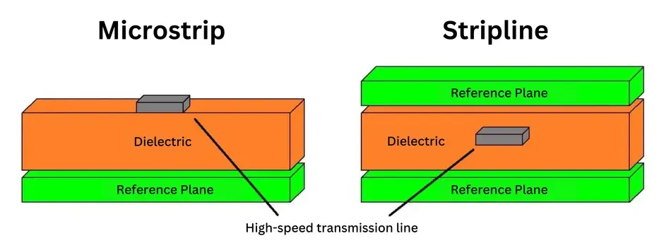
Transmission line theory forms the foundation of impedance control in PCBs. A PCB trace acts as a distributed transmission line when signal rise times are short relative to propagation delay, typically beyond 100 MHz. The characteristic impedance derives from inductance per unit length (L') and capacitance per unit length (C'), where Z0 = sqrt(L'/C'). For microstrip lines on the outer layers, air above the trace reduces effective dielectric constant, while striplines embedded between ground planes offer better shielding but demand precise layer spacing.
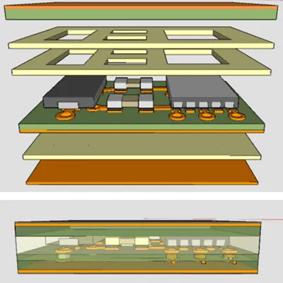
Embedded components introduce unique challenges to these principles. Integrating capacitors or resistors modifies local material properties, creating pockets of varying permittivity that perturb the electromagnetic field around nearby traces. This leads to embedded components impedance fluctuations, potentially shifting Z0 by 5 to 15 percent if unaccounted for. Designers must model these effects using field solvers to predict field distributions and adjust trace geometries accordingly. IPC-2141A provides guidance on calculating impedances for high-speed controlled impedance circuit boards, emphasizing symmetric stackups to minimize variations.
Dielectric materials play a pivotal role, with their constant (Dk) and dissipation factor (Df) directly influencing Z0 and signal loss. Higher Dk materials enable narrower traces for the same impedance but increase crosstalk risk. In embedded designs, resin-coated copper foils or polymer thick films for passives must align with the core laminate's properties. Temperature and humidity also affect Dk, causing drift in Z0 over time, which engineers mitigate through low-loss materials.
Routing geometry further refines control. Trace width and thickness determine inductance, while reference plane proximity sets capacitance. For differential pairs, equal widths and intra-pair spacing maintain balanced impedance. Vias introduce discontinuities, requiring stubs or back-drilling to preserve integrity.
Practical Solutions and Best Practices for Controlled Impedance Routing
Achieving controlled impedance routing starts with stackup design. Engineers should specify symmetric builds with dedicated power and ground planes flanking signal layers to provide continuous return paths. Core and prepreg thicknesses must balance mechanical stability with impedance targets, often iterating via stackup calculators. For embedded components, position passives away from critical high-speed nets or compensate with wider traces nearby.
Material selection demands low-Dk, low-Df laminates stable across frequencies. Hybrid stackups combining high-speed outer layers with cost-effective inners suit mixed-signal boards. Fabrication notes should call out impedance targets, tolerances like ±10 percent, and test coupons for verification.
Routing best practices include length matching for differential signals and avoiding sharp bends, which cause impedance bumps. Orthogonal routing between layers reduces coupling. Engineers employ length-tuning meanders judiciously, ensuring they do not exceed quarter-wavelength at the highest frequency.
Manufacturing processes must align with design intent. Etch tolerances, plating uniformity, and solder mask effects alter final Z0, so communicate stackup details early. IPC-2221C outlines generic requirements for printed board design, including conductor sizing for controlled impedance. Post-fabrication, time-domain reflectometry (TDR) confirms compliance, plotting impedance profiles along traces.
In assembly, reflow profiles per IPC-6012E ensure dimensional stability, preserving impedance after thermal stress. Electrical engineers benefit from partnering with fabricators experienced in impedance-controlled panels.
Challenges and Troubleshooting in Embedded Component PCBs
Embedded designs face warpage from CTE mismatches between components and substrates, distorting layer spacing and thus impedance. Troubleshooting involves finite element analysis to predict bow and twist, followed by constrained lamination. Signal probing reveals discontinuities; correlate with cross-sections to identify via stubs or etch variations.
Crosstalk arises from inadequate spacing near embedded passives. Increase separation or add ground stitching vias. Humidity absorption swells dielectrics, shifting Z0; bake boards pre-assembly and use moisture-resistant materials.
Conclusion
Impedance control PCB practices are vital for optimizing signal transmission in embedded component PCBs. By mastering characteristic impedance principles, stackup design, and controlled impedance routing, engineers ensure superior signal integrity. Adhering to standards like IPC-2141A, IPC-2221C, and IPC-6012E minimizes risks from manufacturing variations and component integration. These strategies enable reliable high-speed performance, paving the way for compact, efficient electronics.
FAQs
Q1: What factors most affect characteristic impedance in transmission line PCBs with embedded components?
A1: Characteristic impedance depends on trace width, copper thickness, dielectric height, and material Dk. Embedded components locally alter these by changing permittivity, requiring field solver adjustments. Maintain symmetric stackups and test with TDR for verification. Follow IPC-2141A guidelines to predict and control variations effectively.
Q2: How does controlled impedance routing improve signal integrity in high-speed designs?
A2: Controlled impedance routing matches trace Z0 to driver and receiver, preventing reflections and distortion. In embedded component PCBs, it counters dielectric discontinuities for cleaner eye diagrams. Use differential pairs with tight tolerances and reference planes to reduce crosstalk. This approach sustains data rates beyond 10 Gbps reliably.
Q3: What are common tolerances for impedance control PCB fabrication?
A3: Typical tolerances range from ±10 percent for standard boards to ±5 percent for precision high-speed nets. Factors like etch control and plating uniformity influence achievability. Specify test coupons and TDR limits in fab notes. Electrical engineers verify post-production to ensure transmission line PCB integrity.
Q4: Why is stackup symmetry critical for embedded components impedance management?
A4: Symmetry ensures uniform dielectric spacing, stabilizing Z0 across layers. Asymmetric builds cause warpage and field imbalances near embedded passives. Design mirrored cores and prepregs per IPC-2221C. This practice optimizes signal transmission and mechanical reliability.
References
IPC-2141A — Design Guide for High-Speed Controlled Impedance Circuit Boards. IPC, 2004
IPC-2221C — Generic Standard on Printed Board Design. IPC, 2023
IPC-6012E — Qualification and Performance Specification for Rigid Printed Boards. IPC, 2017