Introduction
Effective grounding in printed circuit board (PCB) design is a cornerstone of reliable and high-performing electronic systems. For electrical engineers, mastering PCB grounding techniques ensures minimal noise, reduced electromagnetic interference (EMI), and enhanced signal integrity. Grounding issues can lead to system failures, data corruption, or safety hazards if not addressed. This article explores proven strategies such as single point grounding, multi-ground strategy, shortened connections, and placing bypass caps to optimize your designs. By understanding and applying these methods, you can elevate the performance of your circuits and meet stringent industry standards. Whether working on low-frequency analog or high-speed digital systems, grounding remains a critical factor. Let us dive into the principles and practices that define effective grounding for modern PCB layouts.
What Is PCB Grounding and Why It Matters
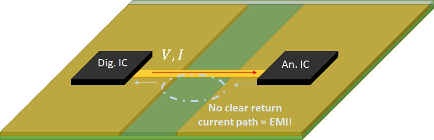
PCB grounding refers to the process of creating a low-impedance path for electrical currents to return to their source, typically through a ground plane or dedicated traces. This technique stabilizes voltage levels, minimizes noise, and protects components from stray currents or static discharges. Grounding is vital for maintaining signal integrity, especially in mixed-signal or high-frequency designs where interference can degrade performance. Poor grounding can result in crosstalk, ground loops, or EMI issues, leading to erratic behavior in sensitive circuits. For electrical engineers, proper grounding is not just a design choice but a necessity to comply with safety and performance standards like those outlined in IPC-6012E. Without it, even the most advanced designs risk failure under real-world conditions. Grounding directly impacts the reliability and efficiency of electronic systems across industries.
Technical Principles of PCB Grounding
Grounding in PCB design operates on fundamental electrical principles aimed at controlling current flow and minimizing interference. The primary goal is to provide a reference point for voltages and a safe path for fault currents. A well-designed ground system reduces the potential difference between components, preventing noise from coupling into signals. Key concepts include impedance control, where the ground path must have minimal resistance and inductance to handle transient currents effectively. Ground loops, caused by multiple ground paths, can introduce unwanted noise, especially in analog circuits. Frequency also plays a role, as high-frequency signals require careful management of return paths to avoid EMI. Standards such as IPC-A-600K emphasize the importance of consistent ground plane implementation to ensure performance. Understanding these principles allows engineers to tailor grounding strategies to specific circuit requirements and operational environments.
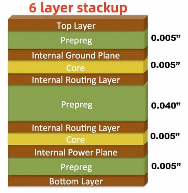
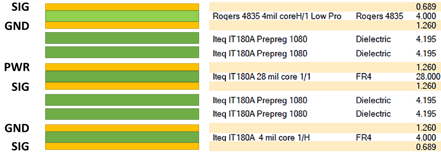
Ground Planes and Their Role
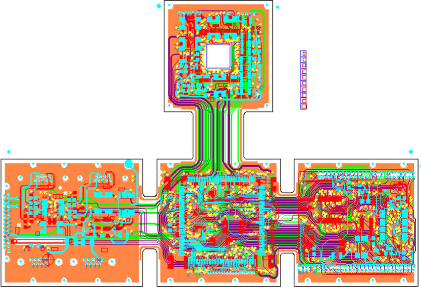
A ground plane is a large conductive area on a PCB layer, often copper, dedicated to grounding. It serves as a common reference point and reduces impedance for return currents. Ground planes are essential in high-speed designs to provide a stable path for signals and minimize EMI. They also act as a shield, reducing crosstalk between adjacent traces. Implementing a solid ground plane, as recommended by industry guidelines like IPC-6012E, enhances overall circuit stability. Engineers must ensure the ground plane is uninterrupted by slots or cuts, which can disrupt current flow and increase noise. Proper connection of components to this plane is critical for maintaining low-impedance paths across the board.
Single Point Grounding Explained
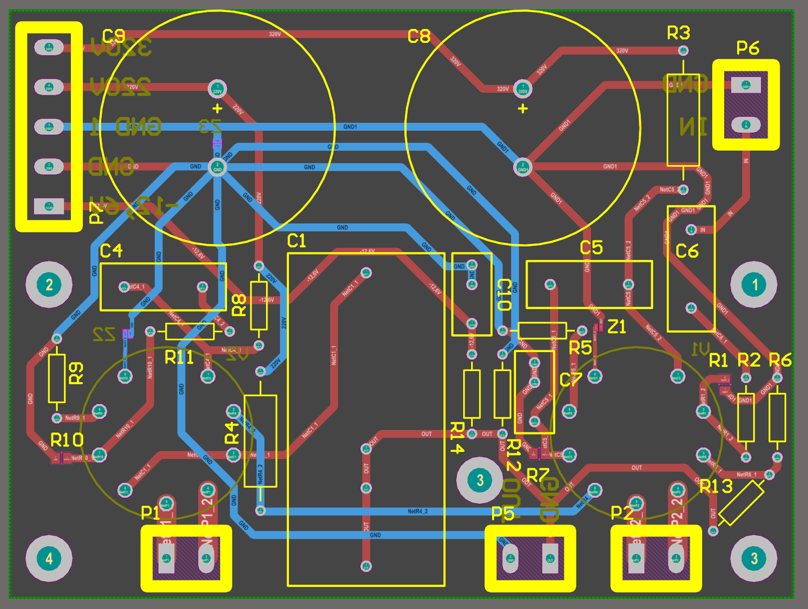
Single point grounding involves connecting all ground references to one common point on the PCB. This technique prevents ground loops by ensuring there is only one return path for currents. It is particularly effective in low-frequency or analog circuits where noise sensitivity is high. By centralizing the ground connection, potential differences between circuit sections are minimized. However, single point grounding may not suit high-frequency designs due to increased impedance over long traces. Careful placement of the grounding point, often near the power supply return, is necessary to optimize performance. This method aligns with best practices in standards like IPC-A-600K for reducing interference in sensitive applications.
Multi-Ground Strategy for Complex Designs
In contrast, a multi-ground strategy involves using multiple ground planes or points tailored to different circuit sections, such as analog and digital domains. This approach is common in mixed-signal designs where separating noisy and sensitive grounds prevents interference. Each ground type connects to a main ground point, often through controlled paths like inductors or resistors, to manage current flow. A multi-ground strategy requires meticulous planning to avoid unintended coupling between sections. It is effective for high-speed systems but demands precise layout to maintain isolation. Following guidelines from IPC-6012E ensures that multi-ground implementations meet performance and safety criteria in complex PCB layouts.
Suggested Reading: PCB Grounding Techniques: A Guide to Minimizing Noise and Ensuring Reliable Connections
Practical Solutions and Best Practices
Implementing effective grounding techniques requires a combination of theoretical understanding and practical application. Electrical engineers can adopt several strategies to enhance PCB performance through grounding. These methods address common challenges like noise, EMI, and signal distortion while adhering to industry standards. Below are actionable approaches focusing on single point grounding, multi-ground strategy, shortened connections, and placing bypass caps to achieve optimal results in your designs.
Implementing Single Point Grounding
To apply single point grounding, identify a central location for all ground connections, typically near the power supply input. Connect all circuit grounds to this point using dedicated traces or vias. Avoid creating multiple paths that could form loops and introduce noise. This technique works well for low-frequency circuits or systems with minimal current transients. Ensure the grounding point is robust enough to handle the total return current without voltage drops. Regularly inspect the layout for compliance with standards like IPC-A-600K to maintain design integrity.
Optimizing with Multi-Ground Strategy
For a multi-ground strategy, segregate grounds based on circuit function, such as digital, analog, and power grounds. Use separate planes or traces for each type and connect them at a single point to prevent interference. Place isolation components like ferrite beads between ground domains to filter noise. Ensure clear labeling in the layout to avoid mix-ups during assembly. This method suits complex designs with varying noise levels across sections. Refer to IPC-6012E for guidance on maintaining separation and connection integrity in multi-ground setups.
Shortened Connections for Reduced Impedance
Shortened connections are critical to minimizing impedance in ground paths, especially at high frequencies. Design ground traces or vias as short as possible to reduce inductance and resistance. Position components close to ground points or planes to limit trace length. In high-speed designs, avoid long meandering paths that can act as antennas, radiating EMI. Use multiple vias to connect to ground planes for redundancy and lower impedance. This practice enhances signal integrity and aligns with best practices in high frequency PCB design standards like IPC-6012E.
Placing Bypass Caps for Noise Suppression
Placing bypass caps, also known as decoupling capacitors, near power pins of active components is essential for noise suppression. These capacitors filter high-frequency noise by providing a local energy reservoir, stabilizing voltage levels. Position them as close as possible to the pins they serve, ideally within a few millimeters, to minimize lead inductance. Use appropriate capacitance values based on the frequency range of the circuit. Multiple capacitors of different values can address a broader noise spectrum. Ensure proper connection to ground planes through low-impedance paths. This technique, supported by guidelines in IPC-A-600K, significantly reduces power supply noise.
Additional Grounding Tips
Beyond these core techniques, consider filling unused PCB areas with ground pours to enhance EMI shielding and heat dissipation. Avoid splitting ground planes unnecessarily, as it can disrupt return paths. Route high-current traces away from sensitive analog sections to prevent interference. Regularly simulate layouts using appropriate tools to identify potential grounding issues before fabrication. Adhering to standards like IPC-6012E ensures that these practices contribute to a robust and reliable design.
Troubleshooting Grounding Issues
Grounding problems often manifest as noise, signal distortion, or unexpected system behavior. Start by checking for ground loops using a multimeter to measure potential differences across ground points. If loops exist, consolidate connections to a single point or isolate domains using a multi-ground strategy. Inspect trace lengths and ensure shortened connections to minimize impedance, particularly in high-frequency sections. Verify that bypass caps are correctly placed and sized for the application. Use oscilloscopes to detect noise on power lines, adjusting capacitor placement if needed. Review the layout against standards like IPC-A-600K to confirm compliance. Systematic troubleshooting helps identify and resolve grounding issues, ensuring stable circuit operation in demanding environments.
Conclusion
Mastering PCB grounding techniques is essential for electrical engineers aiming to create reliable and efficient electronic systems. Strategies like single point grounding, multi-ground strategy, shortened connections, and placing bypass caps offer tailored solutions to diverse design challenges. By understanding the principles behind grounding and applying best practices, you can significantly reduce noise, EMI, and signal integrity issues. Grounding is not a one-size-fits-all approach, it requires careful consideration of circuit type, frequency, and layout constraints. Adhering to recognized standards ensures that your designs meet performance and safety benchmarks. Implementing these methods will enhance your PCB designs, leading to robust and dependable products across various applications.
FAQs
Q1: What are the benefits of single point grounding in PCB design?
A1: Single point grounding offers a simple way to prevent ground loops by connecting all grounds to one location. This reduces noise in low-frequency or analog circuits by minimizing potential differences. It is easy to implement and suits less complex designs. However, it may not be ideal for high-frequency systems due to increased impedance over longer traces. Following industry standards ensures its effectiveness in suitable applications.
Q2: How does a multi-ground strategy improve mixed-signal PCB performance?
A2: A multi-ground strategy enhances mixed-signal PCB performance by separating analog and digital grounds to prevent noise coupling. Each ground type connects at a controlled point, maintaining isolation between domains. This approach manages interference effectively in complex designs. Proper implementation, guided by recognized standards, ensures signal integrity and reduces EMI in systems with diverse circuit functions.
Q3: Why are shortened connections important for high-frequency PCB designs?
A3: Shortened connections are vital in high-frequency PCB designs to minimize impedance and inductance in ground paths. Long traces can act as antennas, radiating EMI and degrading signal quality. Keeping connections short, often with multiple vias, ensures low-impedance return paths. This practice supports stable operation and aligns with guidelines for high-speed circuit layouts, enhancing overall performance.
Q4: What is the role of placing bypass caps in noise reduction?
A4: Placing bypass caps near power pins of components filters high-frequency noise by providing a local energy source. This stabilizes voltage and prevents fluctuations from affecting circuit operation. Positioning them close to pins minimizes inductance, improving effectiveness. Using multiple values can address various noise frequencies. This technique significantly enhances power integrity in PCB designs when applied correctly.
References
IPC-6012E — Qualification and Performance Specification for Rigid Printed Boards. IPC, 2020.
IPC-A-600K — Acceptability of Printed Boards. IPC, 2020.