Why PCB Thermal Management is Essential for Electronic Reliability
In the rapidly evolving landscape of Printed Circuit Board (PCB) design, effectively managing heat is a paramount concern. As electronic devices continue to shrink in size while simultaneously increasing in power and functionality, robust PCB thermal management becomes critical not only for maintaining optimal performance but also for preventing premature failures. Excessive temperatures are a primary antagonist for electronic components, leading to performance degradation, outright component failure, and a reduced operational lifespan for the entire device.
For high-power applications—such as advanced power supplies, sophisticated automotive electronics, and high-intensity LED systems—thermal control is even more crucial. Inadequate PCB thermal management can result in undesirable thermal stress, board warping, or even complete system shutdowns. Consequently, a deep understanding of how heat propagates through a PCB, especially through its inner layers, is vital for both engineers and designers. While outer layers typically interface with ambient air or external heatsinks, inner layers predominantly rely on their material properties, particularly copper thickness, to efficiently transfer heat away from critical components.
The Core Principles of Heat Dissipation in PCBs
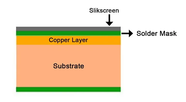
Heat dissipation within a fast turn custom PCB occurs primarily through three mechanisms: conduction, convection, and radiation. Among these, conduction—the transfer of thermal energy directly through a material—is the dominant mode within the PCB structure itself. Copper is an exceptional thermal conductor, boasting a thermal conductivity of approximately 401 W/m·K, making it the material of choice for effectively spreading heat across the board's surface and through its internal layers.
Inner Layers as Heat Spreaders
In a multilayer PCB, the inner copper layers function as crucial heat spreaders. When an active component generates heat, this thermal energy is efficiently conducted through these copper layers. From there, it is ultimately dissipated to the surrounding environment, either through convection (natural or forced air cooling) or by radiation. The overall efficiency of this heat transfer process is profoundly influenced by the thickness of the copper within these inner layers. Thicker copper provides a significantly larger cross-sectional area, creating a lower thermal resistance path for heat flow. This enhanced conductivity directly translates to superior inner layer heat dissipation.
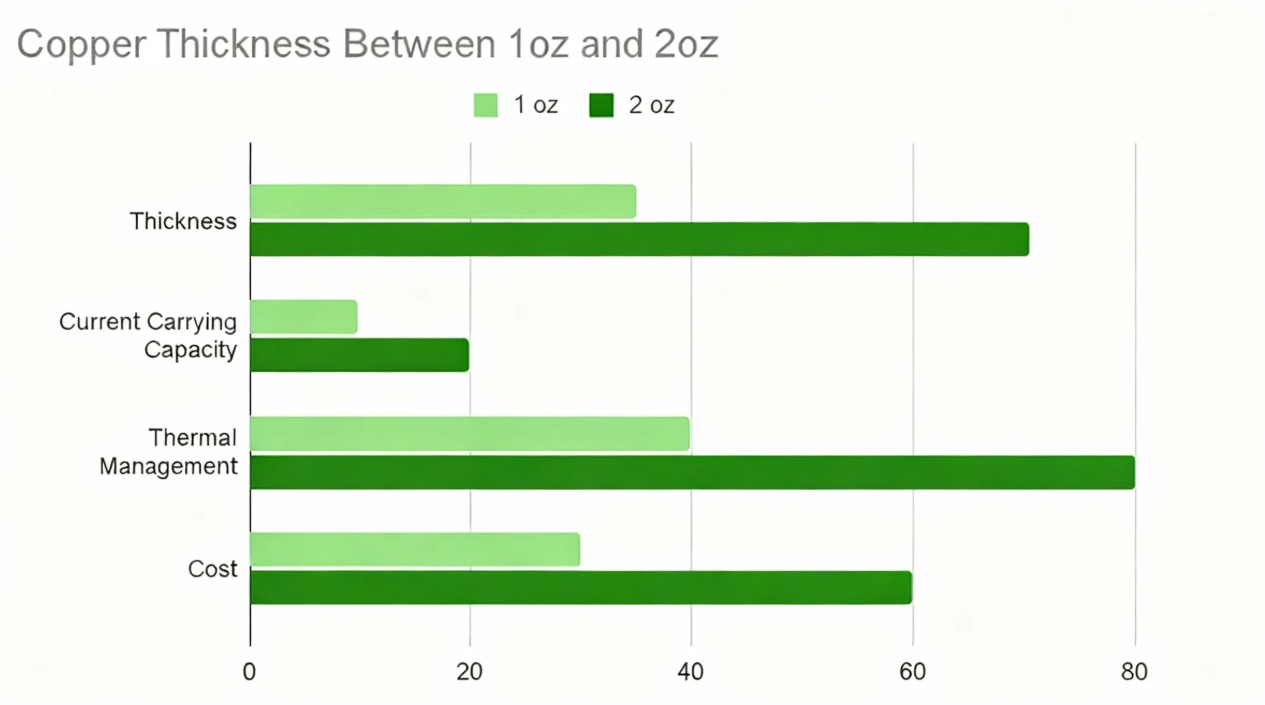
For instance, a standard copper thickness of 1 ounce per square foot (1 oz/ft²), equating to about 35 micrometers, might suffice for circuits with low power demands. However, in designs incorporating high-power elements, increasing the inner layer copper to 2 oz/ft² (70 micrometers) or even 3 oz/ft² (105 micrometers) can lead to a substantial reduction in temperature rise. Based on typical thermal simulations for power electronics, such an increase can lower the operating temperature under heavy loads by as much as 10-20°C, significantly improving reliability.
How Copper Thickness Directly Influences Temperature
The correlation between inner layer copper thickness and operating temperature is quite direct: employing thicker copper layers effectively reduces the overall thermal resistance of the PCB. This reduction enables heat to spread more uniformly across the board, thereby preventing the formation of localized hotspots. Thermal resistance, typically measured in degrees Celsius per watt (°C/W), quantifies how much a temperature rises for a given amount of power being dissipated. A lower thermal resistance value unequivocally indicates superior heat dissipation capabilities.
Performance Gains vs. Design Trade-offs
Consider a scenario where a power integrated circuit (IC) dissipates 5 watts of heat. With a 1 oz/ft² copper layer, the temperature rise might be around 50°C above ambient, depending on the specific board layout and surrounding airflow. By enhancing the inner layer copper to 2 oz/ft², this temperature rise could realistically decrease to 30-35°C due to the improved heat spreading capacity. Such a reduction is often critical for preventing thermal failures, especially in compact designs where space for additional cooling solutions is severely limited.
However, the strategy of simply increasing copper thickness isn't without its caveats. Thicker copper inevitably escalates manufacturing costs and can introduce complexities in the etching process, particularly for designs with very fine traces. Furthermore, beyond a certain thickness—typically in the range of 3-4 oz/ft²—the additional benefits gained from further increasing copper mass tend to diminish. This is because other limiting factors, such as the thermal properties of the dielectric material or the overall board size, begin to dominate the thermal performance. Therefore, achieving an optimal balance between manufacturing cost and thermal performance is paramount when determining copper thickness for effective PCB thermal management.
Inner Layers in Multilayer PCBs: Critical Heat Paths
In the architecture of multilayer PCBs, inner layers frequently serve as dedicated power or ground planes. These expansive, continuous copper planes provide a significantly large surface area that is ideal for efficient heat spreading. Unlike the often narrow and fragmented signal traces found on outer layers, inner planes, when designed with adequate copper thickness, can function as highly effective internal heat sinks.
For example, a 4-layer PCB configured with 2 oz/ft² copper for its inner power and ground planes can manage substantially more heat than an equivalent board using only 1 oz/ft² copper. These robust inner layers efficiently distribute heat across the entire board, mitigating the risk of localized overheating in close proximity to high-power components. This characteristic is particularly vital in applications such as motor control circuits or RF amplifiers, where heat generation is often concentrated within specific, small areas. A practical recommendation is to maximize the copper area on these inner layers by minimizing any cutouts or deliberate splits within the power and ground planes. A solid, unbroken plane offers the lowest thermal resistance, ensuring the best possible inner layer heat dissipation. If routing constraints necessitate splits, consider incorporating thermal bridges—small copper connections across these splits—to maintain a continuous pathway for heat flow.
Boosting Heat Dissipation with Thermal Vias
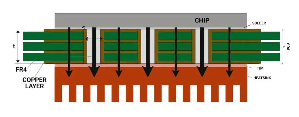
While optimized copper thickness is a major contributor to lateral heat spreading, it's not the sole component in effective PCB cooling. Thermal vias represent another potent technique to significantly enhance heat transfer, especially within multilayer board structures. These are small, plated holes that establish direct thermal pathways, connecting inner copper layers to outer layers or, in some cases, directly to an external heatsink. Their primary function is to facilitate the vertical movement of heat through the PCB.
Thermal vias operate by providing a low-resistance conduit, allowing heat to escape efficiently from the inner layers to the board's surface. Once at the surface, this heat can then be effectively dissipated via convection (through airflow) or by conduction to an attached heatsink. For maximum effectiveness, thermal vias should be strategically placed directly beneath the primary heat-generating components, such as power transistors or integrated circuits (ICs). A common design approach involves an array of vias, perhaps 0.3 mm in diameter with a 1.2 mm spacing, often filled with copper to further augment their thermal conductivity. Combining these thermal vias with thicker inner copper layers creates a highly robust and comprehensive thermal management system. The thick copper spreads heat horizontally, while the vias efficiently transfer it vertically to areas where it can be most effectively dissipated. Studies have consistently shown that integrating thermal vias can reduce component temperatures by 10-15°C in high-power designs, with the precise reduction depending on factors like via density and their strategic placement.
Complementary PCB Cooling Methodologies
Beyond the fundamental strategies of optimizing copper thickness and employing thermal vias, a variety of other PCB cooling techniques can synergistically enhance your overall thermal management efforts. Implementing these approaches alongside core design principles ensures a comprehensive heat dissipation solution.
Additional Cooling Strategies
● Strategic Component Placement: Thoughtful positioning of components can significantly impact thermal performance. High-power components should be placed away from each other to prevent the formation of concentrated heat zones. Positioning them near board edges or in areas with superior airflow can leverage natural convection for more efficient cooling.
● Heatsinks and Thermal Interface Materials: Attaching heatsinks directly to critical, high-power components is a direct method of heat removal. Concurrently, utilizing thermal pads or thermal paste improves the heat transfer efficiency from the component to the heatsink. The PCB layout must accommodate the proper mounting and clearance for these crucial cooling aids.
● Advanced Board Material Selection: For applications demanding extreme heat management, such as high-power LED lighting, consider employing substrates with inherently higher thermal conductivity, like metal-core PCBs (MCPCBs). While standard FR-4 material possesses a relatively low thermal conductivity (around 0.3 W/m·K), aluminum-backed boards can offer significantly higher values, often exceeding 2 W/m·K.
● Optimized Airflow Design: In systems that incorporate forced air cooling (fans), the PCB layout should be meticulously designed to align with and facilitate the intended airflow patterns. This ensures that the generated heat is efficiently carried away from the board, preventing recirculation and promoting effective cooling.
Integrating these diverse techniques with optimized copper thickness creates a balanced and highly effective design that maximizes both performance and long-term reliability by addressing every aspect of heat dissipation.
Practical Design Considerations for Inner Layer Copper
Designing a PCB for optimal heat dissipation demands meticulous planning and foresight. Here are actionable tips to guide your decision-making when considering the interplay between copper thickness and operational temperature.
Key Design Tips
● Early Power Requirement Assessment: During the initial schematic design phase, identify all high-power components and accurately estimate their expected heat output. This crucial data should directly inform your decisions regarding the inner layer copper thickness well before the physical layout process begins.
● Leverage Simulation Software: Utilize advanced thermal simulation software to accurately model heat flow within your PCB design. These tools can predict temperature rises based on chosen copper thickness, thermal via placement, and material properties, thereby saving valuable development time and minimizing costly design revisions.
● Strategic Cost-Performance Balance: While thicker copper (e.g., 2-3 oz/ft²) demonstrably enhances inner layer heat dissipation, it inherently increases production costs. Therefore, apply thicker copper strategically, typically in power planes adjacent to significant heat sources, while opting for standard thickness (e.g., 1 oz/ft²) in less thermally critical areas.
● Collaborate with Manufacturers: Establish close communication with your PCB fabrication partner. Understand their specific capabilities and limitations concerning various copper thicknesses and thermal via filling techniques. This proactive collaboration ensures that your design is manufacturable without encountering unexpected production issues.
Challenges and Constraints of Utilizing Thicker Copper Layers
While the advantages of employing thicker copper for PCB thermal management are clear, this approach is not without its trade-offs. A comprehensive understanding of these challenges is essential for making well-informed design decisions that balance performance with practical considerations.
Inherent Limitations
● Manufacturing Complexity: Thicker copper requires extended etching times during fabrication. This can lead to increased undercutting, which may compromise the precision and fine detail of traces, particularly in high-density designs with tight tolerances.
● Increased Production Costs: The overall cost of manufacturing a PCB directly correlates with the copper thickness. This rise is due to higher material consumption and more extensive processing times, which can significantly impact project budgets, especially for large-scale production runs.
● Weight and Physical Size: Incorporating thicker copper adds noticeable weight to the PCB. This can be a significant concern in weight-sensitive or portable applications, such as drones, wearable devices, or compact handheld electronics, where every gram matters.
● Diminishing Returns: Beyond a certain threshold (typically around 3-4 oz/ft²), further increases in copper thickness provide only marginal improvements in heat dissipation. At this point, other factors, such as the effectiveness of external heatsinks, airflow, or the thermal properties of the dielectric materials, often become the primary limiting factors for overall thermal performance.
Designers must carefully weigh these inherent limitations against the anticipated thermal benefits to create a PCB design that is both cost-effective and thermally efficient, tailored to the specific application's requirements.
Conclusion: Mastering PCB Thermal Management with Inner Layer Design
Effective PCB thermal management stands as a cornerstone of reliable electronic design, and the critical role played by inner layer heat dissipation cannot be overemphasized. By judiciously selecting the appropriate copper thickness, strategically incorporating thermal vias, and intelligently applying complementary PCB cooling techniques, designers can significantly reduce operational temperature rises. This proactive approach not only enhances the performance of electronic devices but also considerably extends their operational lifespan. The intricate relationship between copper thickness and temperature is a pivotal factor—where thicker copper efficiently lowers thermal resistance and uniformly spreads heat—however, this must always be balanced against practical considerations such as manufacturing cost and design constraints.
Regardless of whether you are designing for high-power industrial systems or compact consumer electronics, comprehending and optimizing the copper thickness within your inner layers is an indispensable asset for effectively tackling thermal challenges. Equipped with the insights and practical strategies shared in this guide, you are well-prepared to engineer thermally efficient PCB designs that will robustly withstand the demands of even the most rigorous applications.