Introduction
In the world of printed circuit board manufacturing, inner layer copper thickness plays a pivotal role in ensuring PCB reliability under demanding operational conditions. Engineers often specify copper weights like 1 oz per square foot, but achieving the finished thickness after processing requires adherence to precise inner layer standards. IPC-6011 copper thickness guidelines set the foundation for generic performance, while specifics for rigid boards come from related documents. Non-compliance can lead to issues such as signal integrity loss, thermal failures, or mechanical weaknesses. This article breaks down copper weight requirements and PCB compliance essentials from a factory perspective. Understanding these helps electric engineers design boards that withstand real-world stresses without over-specifying.
Understanding Inner Layer Copper Thickness and Its Role in PCB Reliability
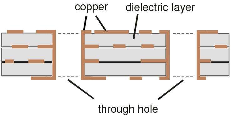
Inner layers in multilayer PCBs carry signals and power between outer surfaces, making their copper thickness critical for current handling and interlayer adhesion. Copper weight, expressed in ounces per square foot, translates to nominal foil thicknesses before processing: 0.5 oz equals about 17 microns, 1 oz around 35 microns, and 2 oz roughly 70 microns. During lamination and etching, inner layer copper experiences reductions, so finished thicknesses must meet minimums to maintain PCB reliability. Factory processes like oxide treatment and etching can remove up to 20-30% of the foil, depending on the pattern density. Inner layer standards ensure these layers resist delamination and electromigration over time. For high-reliability applications, such as power electronics, thicker inner copper directly correlates with better thermal dissipation and mechanical integrity.
Key Technical Principles Behind Copper Thickness Specifications
Copper thickness influences trace resistance, where thinner foils increase ohmic losses, potentially causing hotspots in high-current paths. In multilayer boards, inner layers lack direct cooling, so IPC standards emphasize minimum finished thicknesses to support current capacities per IPC-2152 guidelines, though focused here on structural specs. Etching uniformity is vital; over-etching narrow traces thins copper disproportionately, risking opens or voids. Adhesion to the dielectric relies on sufficient foil weight, as thin inner layers peel under thermal cycling. Fabrication tolerances account for these, with inner copper verified via cross-section analysis post-process. Balancing copper weight requirements prevents warpage, as asymmetric thicknesses across layers induce bow and twist during reflow.
IPC Standards for Inner Layer Copper: Breaking Down the Requirements
IPC-6012 provides detailed tables for finished copper thicknesses after processing, with Table 3-13 outlining internal layer minimums applicable across classes. For a starting 1 oz foil on inner layers, the minimum finished thickness is 25 microns, ensuring reliability without plating additions. Similarly, 0.5 oz starts yield at least 12 microns finished, while 2 oz requires 56 microns minimum. These values reflect etching losses and apply to rigid boards under IPC-6011 generic performance umbrellas. IPC-A-600 complements by defining acceptability, rejecting boards below these thresholds via visual and microscopic checks. Copper weight requirements thus guide laminate selection, with factories panel-plating cores to hit targets precisely.
External layers differ, gaining 20-25 microns from panel plating, but inner layers depend solely on starting foil quality. Class 3 demands tighter controls for aerospace or medical PCBs, though inner mins remain consistent. Engineers specifying IPC-6011 copper thickness must note these as finished values, not starting. Non-conformance often stems from misreading nominal vs. minimum, leading to redesigns. Factories use statistical process control to maintain these inner layer standards.
Best Practices for Achieving PCB Compliance in Inner Layer Copper
Select starting copper weights with 20% margin over minimums to buffer etching variations, especially for fine-pitch designs. Communicate "finished copper thickness" explicitly in fab drawings to align with IPC copper weight requirements. Use heavy oxide or alternative treatments to enhance inner layer adhesion without excessive etchback. Verify via microsection coupons from production panels, targeting averages well above mins for margin. For high-layer-count boards, symmetrize copper weights across cores to minimize warpage risks. Regular audits against IPC-6012 ensure ongoing PCB compliance.
In power PCBs, opt for 2 oz inner planes where current exceeds 5A per trace, calculating widths via derated charts. Avoid mixing weights without dielectric adjustments, as it affects impedance. Prototype with cross-sections early to validate processes.
Common Challenges and Troubleshooting in Inner Layer Fabrication
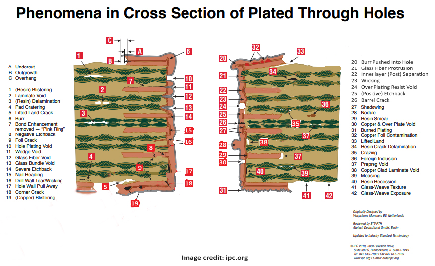
Thin inner copper often results from aggressive etching, manifesting as high resistance or delamination post-lam. Factories troubleshoot by adjusting developer strength and conveyor speed, targeting uniform sidewall profiles. Voids from poor oxide coverage cause reliability failures; inspect cores pre-lam with AOI. Warpage from imbalanced thicknesses requires sequential lamination or carrier panels. If microsections show below 25 microns on 1 oz inners, revert to thicker starts or refine etch factors. These align with inner layer standards, preventing field returns.
Over-thick copper wastes material and complicates drilling; cap at nominals unless specified. Thermal stress tests per IPC-TM-650 confirm integrity.
Conclusion
Mastering inner layer copper thickness requirements demystifies IPC standards, directly boosting PCB reliability and compliance. From 25-micron mins for 1 oz to proportional scalings, these specs balance performance with manufacturability. Factory-driven adherence to IPC-6012 and IPC-A-600 ensures boards endure cycles without compromise. Electric engineers benefit by specifying finished values upfront, incorporating margins, and validating via sections. Prioritizing these copper weight requirements yields robust multilayers ready for assembly and deployment.
FAQs
Q1: What are the minimum IPC-6011 copper thickness values for inner layers?
A1: IPC-6011 copper thickness aligns with generic specs, but rigid boards follow IPC-6012 Table 3-13: 12 microns for 0.5 oz starting, 25 microns for 1 oz, and 56 microns for 2 oz finished on inners. These ensure PCB reliability by accounting for etching losses. Factories measure via cross-sections to confirm compliance across classes.
Q2: How does inner layer copper affect PCB reliability?
A2: Insufficient inner copper thickness reduces current capacity and adhesion, leading to electromigration or delamination under thermal stress. Standards mandate mins to support signal integrity and mechanical strength in multilayers. Proper copper weight requirements prevent hotspots, enhancing long-term PCB reliability.
Q3: What are common copper weight requirements for inner layers in Class 3 PCBs?
A3: Class 3 inner layer standards per IPC-6012 require the same minimum finished thicknesses as lower classes: 25 microns for 1 oz foil post-process. Focus on verification to meet PCB compliance. Engineers should specify starting weights accordingly for high-reliability apps.
Q4: How to ensure PCB compliance with inner layer standards during fabrication?
A4: Specify finished copper thicknesses in drawings, use process controls for etching, and test coupons per IPC-A-600. This upholds IPC-6011 copper thickness and overall standards. Regular microsections confirm adherence to copper weight requirements.
References
IPC-6012 — Qualification and Performance Specification for Rigid Printed Boards. IPC
IPC-A-600 — Acceptability of Printed Boards. IPC
IPC-6011 — Generic Performance Specification for Printed Boards. IPC