Introduction
Laser drilling has become a cornerstone in modern PCB manufacturing, particularly for high-density interconnect (HDI) designs that demand microvias smaller than traditional mechanical methods can achieve. As electric engineers evaluate PCB manufacturing costs, understanding the laser drilling cost becomes essential for balancing performance and budget in projects involving fine-pitch components or compact form factors. This process enables precise vias with diameters as small as 50 microns, supporting advanced applications like smartphones, medical devices, and aerospace electronics. However, the initial investment in laser drilling raises questions about its return on investment (ROI), especially when compared to conventional drilling techniques. Factory-driven insights reveal that while laser drilling elevates upfront expenses, it often delivers long-term savings through higher yields and design flexibility. This article dissects the laser drilling cost factors, microvia cost analysis, and practical strategies to determine if it justifies inclusion in your PCB project.
What Is Laser Drilling and Why Does It Matter for PCB Costs?
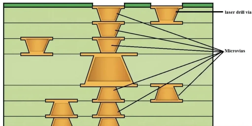
Laser drilling uses a focused beam of light, typically CO2 or UV lasers, to ablate material and create vias without physical contact, distinguishing it from mechanical drilling that relies on rotating bits. In PCB production, it excels at forming blind, buried, or stacked microvias essential for HDI structures, where via sizes below 150 microns are common. This capability matters because mechanical drilling struggles with aspect ratios exceeding 10:1 for small diameters, leading to tapered holes and reliability issues in dense boards. For electric engineers, the relevance ties directly to PCB manufacturing cost, as laser drilling supports miniaturization that reduces overall board size and layer count in some designs. Industry standards like IPC-2226 provide guidelines for HDI via design, ensuring compatibility with laser processes to avoid excessive costs from redesigns. Ultimately, ignoring laser drilling in high-density projects can inflate costs through larger boards or performance compromises.
The economic impact stems from how laser drilling shifts cost structures: fixed setup costs are higher due to specialized equipment, but per-via expenses diminish with volume. Factories observe that low-volume prototypes may favor mechanical drilling for affordability, while production runs benefit from lasering's scalability. Microvia cost analysis shows that laser-drilled features enable routing densities unattainable otherwise, potentially cutting material usage and assembly expenses. Engineers must weigh these against tolerances, as laser vias maintain straight walls and minimal heat-affected zones, aligning with quality specs.
Technical Principles of Laser Drilling in PCBs
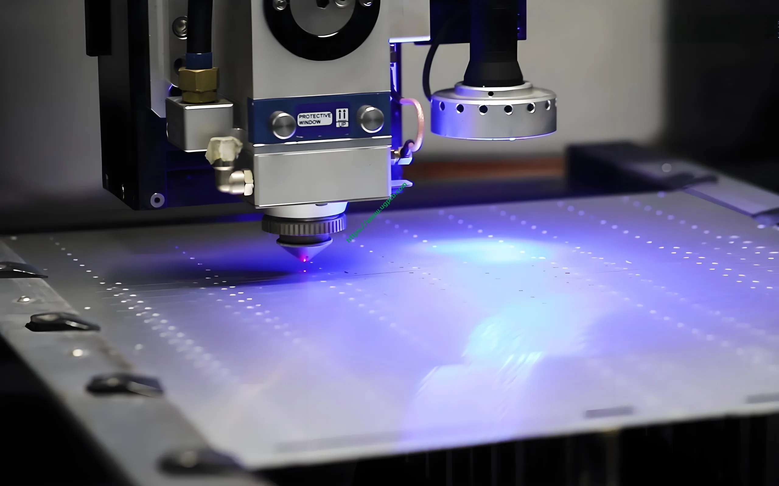
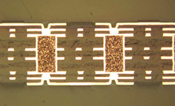
Laser drilling operates on photothermal or photochemical ablation, where the beam's energy vaporizes dielectric and copper layers selectively. CO2 lasers, with wavelengths around 10.6 microns, effectively drill organic dielectrics like FR-4 or resin-coated copper (RCC), while UV lasers handle finer features in advanced materials. The process involves programming the laser's fluence, pulse duration, and scan path to control via depth, typically limited to 1:1 aspect ratios per IPC-6012DS specifications for HDI boards. Precise control prevents carbonization or delamination, critical for subsequent plating and reliability under thermal cycling. Factories calibrate systems for materials' ablation thresholds, ensuring clean entry and exit apertures that meet IPC class 3 requirements.
Beam delivery through galvo mirrors enables rapid positioning, processing thousands of vias per panel without tool wear, unlike mechanical bits that dull quickly on micro-holes. This non-contact method minimizes mechanical stress, reducing warpage in thin cores. However, resin residue requires desmear processes like plasma or permanganate etching, adding steps that influence overall laser drilling cost. Understanding these principles helps engineers specify drill files accurately, optimizing for factory throughput.
Key Factors Affecting Laser Drilling Cost
Several variables drive laser drilling cost in PCB manufacturing, starting with via count and density per panel. High densities increase processing time but leverage the laser's fixed setup, making per-board costs favorable beyond a threshold of several thousand vias. Material selection plays a pivotal role; laser-drillable dielectrics with low ablation energy, such as low-loss resins, process faster than standard FR-4, lowering cycle times. Board thickness and layer buildup affect feasibility, as stacked vias demand multiple sequential drills, escalating expenses.
Via geometry influences costs too: smaller diameters (under 75 microns) require UV lasers, which are slower and pricier than CO2 systems. Factory yields drop with aggressive specs, prompting additional inspections per IPC-A-600 criteria, indirectly hiking PCB manufacturing cost. Panel utilization optimizes economics; nesting more boards reduces waste and amortizes setup. Engineers conducting microvia cost analysis should model these factors early, as fill methods like electroplating or conductive paste add 10-20% more depending on via depth.
Production volume remains the dominant driver for laser drilling ROI. Prototypes incur high relative costs due to amortization over few units, while high-volume runs see costs converge with mechanical drilling. Lead times extend with complex HDI stacks, impacting project timelines.
Laser Drilling vs. Mechanical Drilling: A Cost Perspective
Mechanical drilling suits through-holes and vias over 150 microns, offering lower equipment costs and faster speeds for standard densities. It scales linearly with hit count, as bits wear and require frequent changes, inflating expenses for micro-features. Laser drilling inverts this: high fixed costs from machine depreciation, but negligible incremental per-hole charges, ideal for HDI where mechanical limits apply. Factories report mechanical preferable for simple multilayers, while laser dominates anyvia HDI per IPC-2226 build-up rules.
Hybrid approaches combine both, using mechanical for larger vias and laser for microvias, balancing PCB manufacturing cost. Mechanical introduces smear and breakout issues needing aggressive desmear, while laser's precision cuts post-processing. For electric engineers, crossover occurs around 100-micron vias; below that, laser becomes unavoidable despite premiums.
Microvia Cost Analysis and Laser Drilling ROI
Microvia cost analysis reveals laser drilling's value in enabling HDI classes 4-6, where stacked and staggered vias shrink boards by 30-50% versus standard multilayers. Initial premiums stem from equipment, cleanroom needs, and skilled operation, but ROI materializes through reduced layers, smaller footprints, and higher component density. Calculate laser drilling ROI by comparing total project costs: material savings from fewer layers offset drilling, plus assembly efficiencies from shorter traces lowering signal loss.
Break-even analysis depends on volume; for 1,000+ units, laser often undercuts alternatives by enabling compact designs. Reliability gains per IPC-6012DS reduce field failures, amortizing costs over product life. Engineers should simulate via fanout and escape routing to quantify density benefits against laser drilling cost.
- Via Size Range: Mechanical Drilling >150 μm; Laser Drilling <150 μm
- Cost Scaling: Mechanical Drilling linear (per hit); Laser Drilling fixed + low marginal
- Aspect Ratio: Mechanical up to 10:1; Laser 0.5:1 to 1:1
- Best For: Mechanical suits standard boards; Laser suits HDI microvias
Best Practices for Cost-Effective Laser Drilling
- Select laser-friendly materials early, verifying ablation rates to avoid surprises in production.
- Design vias with IPC-2226 clearances, limiting stacks to three per buildup for yield.
- Optimize drill files by grouping same-depth vias, minimizing head changes and enhancing panel efficiency.
- Collaborate with factories on DfM reviews to flag cost drivers like excessive microvia density.
- Implement sequential buildup cautiously, testing reliability via thermal shock per J-STD-020.
- Monitor desmear efficacy to prevent plating voids.
- Use volume quoting and pilot runs to validate true laser drilling ROI.
Factory Insights: When Laser Drilling Pays Off
In high-volume consumer electronics, laser drilling slashed layer count from 12 to 8, cutting material costs despite via premiums. Aerospace prototypes showed mechanical infeasible for 60-micron vias, forcing laser with positive ROI via weight savings. These cases underscore microvia cost analysis: performance dictates, costs follow.
Conclusion
Laser drilling cost analysis confirms its worth for HDI projects demanding microvias, where PCB manufacturing cost savings emerge from density and reliability. While upfront investments loom large, scalable economics and standard compliance like IPC-6012DS tip scales for volumes over prototypes. Electric engineers achieve optimal laser drilling ROI by factoring via specs, materials, and production scale early. Prioritize DfM to harness precision without excess expense, ensuring project success.
FAQs
Q1: What drives the main differences in laser drilling cost versus mechanical drilling in PCB manufacturing?
A1: Laser drilling incurs higher fixed costs from specialized equipment but lower per-via charges, suiting high-density HDI. Mechanical excels in low-density through-holes with linear scaling tied to bit wear. Material compatibility and desmear add to laser expenses, while mechanical faces limits below 150 microns. Factory insights emphasize volume as the decider for cost efficiency.
Q2: How does microvia cost analysis impact overall PCB project budgeting?
A2: Microvia cost analysis weighs laser drilling premiums against board shrinkage and layer reductions in HDI designs. Smaller vias enable finer routing, potentially halving layers and materials. Yield factors per IPC standards influence totals, with stacks raising complexity. Engineers budget 20-40% more for laser features but recoup via functionality gains.
Q3: When does laser drilling ROI become positive for electric engineers?
A3: Laser drilling ROI turns positive beyond prototype volumes, typically 500-1000 units, as fixed costs distribute. HDI necessities like fine-pitch BGAs justify it regardless, per IPC-2226 guidelines. Compact designs cut assembly and enclosure expenses. Simulate total ownership costs including reliability for accurate assessment.
Q4: What IPC standards guide laser drilling in PCB manufacturing?
A4: IPC-2226 outlines HDI design for microvias, including laser parameters. IPC-6012DS qualifies HDI boards with laser-drilled features. These ensure aspect ratios and tolerances align with factory processes. Adherence minimizes rework and laser drilling cost overruns.
References
IPC-2226 — Design Standard for High Density Interconnect (HDI). IPC, 2003 (with amendments).
IPC-6012DS — Qualification and Performance Specification for High Density Interconnect (HDI) Printed Boards. IPC, 2015.
IPC-A-600K — Acceptability of Printed Boards. IPC, 2020.
J-STD-020E — Moisture/Reflow Sensitivity Classification of Nonhermetic Surface Mount Devices. JEDEC, 2014.