Why a Thoughtful PCB Layout is Crucial for Op-Amp Circuits
Operational amplifiers (op-amps) are fundamental components in analog electronics, powering everything from sophisticated audio equipment to precise sensor interfaces. However, their inherent high gain and sensitivity make them particularly vulnerable to electromagnetic interference (EMI). This interference can severely degrade signal quality, introduce unwanted noise, or cause unpredictable circuit behavior. A poorly designed PCB can inadvertently act as an antenna, picking up and amplifying noise from adjacent digital circuitry, power supplies, or external electromagnetic fields.
The primary objective for engineers is to minimize noise coupling and safeguard signal integrity. A meticulously planned PCB layout helps mitigate parasitic effects, effectively controls ground loops, and provides essential shielding for sensitive signal traces. The following sections will detail specific strategies to combat EMI in op-amp designs, enabling the creation of reliable circuits for even the most demanding applications.
Foundational Principles for Op-Amp PCB Layout
Before delving into advanced methods, it's vital to grasp the core principles that underpin effective op-amp PCB layout guidelines. These rules are universally applicable, whether designing low-frequency audio circuits or high-speed data acquisition systems.
Core Layout Considerations
● Minimize Loop Areas: Shorter, more direct signal and power traces reduce the area available to pick up EMI. Keeping these paths as compact as possible is key.
● Separate Analog and Digital Domains: Improper mixing of analog and digital signals can easily introduce noise. It's imperative to use distinct ground planes and implement careful routing strategies to maintain isolation.
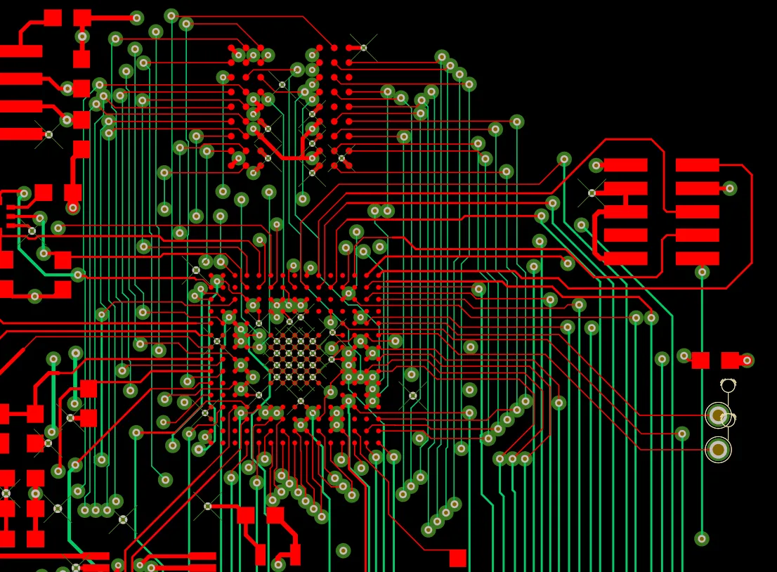
● Prioritize Component Placement: Strategically placing sensitive components, such as op-amps and their associated feedback resistors, in close proximity reduces trace lengths, thereby minimizing parasitic capacitance and susceptibility to noise.
● Implement Robust Grounding: A solid and continuous ground plane is fundamental. It provides a low-impedance return path for currents and offers crucial shielding against EMI.
Proven Techniques for Op-Amp EMI Reduction
EMI can infiltrate op-amp circuits through various conducted or radiated pathways. Here are established EMI reduction techniques for op-amps to effectively suppress noise.
Protecting Sensitive Traces
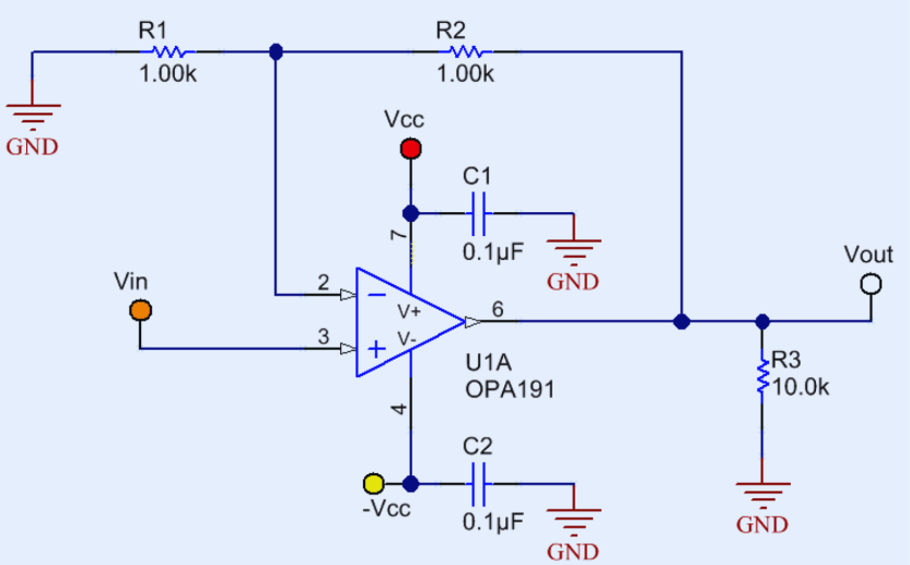
High-impedance nodes, particularly the input pins of an op-amp, are exceedingly susceptible to EMI. To shield these critical points, route their traces away from known noisy areas, such as switching power supplies or high-speed digital lines. When feasible, surround sensitive traces with dedicated ground traces or a solid ground pour to create an effective electromagnetic shield. For example, in a non-inverting amplifier configuration, the input trace to the non-inverting (+) pin should be kept as short as possible and flanked by ground.
Implementing Guard Rings
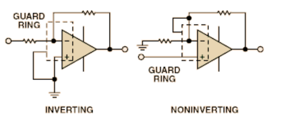
For extremely sensitive applications, such as precision instrumentation, consider integrating a guard ring around the op-amp’s input pins. A guard ring is a conductive trace connected to a low-impedance reference (often ground) that completely encircles the high-impedance input nodes. This design helps intercept stray electric fields before they can couple with and interfere with the delicate signal. Crucially, ensure the guard ring is tied to the exact same potential as the input to prevent the creation of undesirable voltage gradients.
Filtering Power Supply Noise
Noise present on the power supply lines can directly couple into an op-amp’s output, impacting its performance. Employ low-pass filters, typically composed of an RC (resistor-capacitor) or LC (inductor-capacitor) network, on the supply lines to block high-frequency noise components. For instance, a simple filter comprising a 10-ohm resistor in series with a 1 μF capacitor can establish a cutoff frequency around 15.9 kHz, which is often adequate for many low-frequency op-amp applications.
Designing an Effective Op-Amp Ground Plane
The design of the op-amp ground plane is one of the most critical factors for successful EMI reduction. A poorly designed ground system can introduce significant noise, create detrimental ground loops, and severely compromise signal integrity.
The Importance of a Continuous Ground Plane
A solid, unbroken ground plane offers a low-impedance return path for all currents, significantly reducing the potential for EMI. Avoid splitting the ground plane unless absolutely unavoidable, as splits can force return currents to take longer, higher-impedance paths, which inherently introduces noise. For a multilayer PCB, dedicating an entire layer to ground (e.g., in a 4-layer stack-up) ensures the lowest possible impedance—typically less than 0.1 ohms across the plane at lower frequencies.
Star Grounding in Mixed-Signal Environments
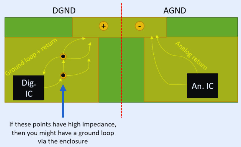
In scenarios involving mixed-signal PCB design for op-amps, where both analog and digital circuits coexist on the same board, implementing a star grounding technique is highly recommended. This method involves connecting all ground points back to a single, central ground node. This prevents fast-switching digital noise from contaminating sensitive analog signals. For example, the ground pins of digital ICs and analog op-amps would connect to separate traces that converge at a common ground point, ideally located near the power supply return.
Avoiding Detrimental Ground Loops
Ground loops arise when return currents have multiple potential paths, leading to voltage differentials that induce noise. To effectively prevent these, ensure that all components within the analog section reference the same precise ground point. If it becomes necessary to segment ground planes (e.g., separate analog and digital grounds), ensure they are connected at a single, carefully chosen point to maintain a unified and stable ground reference.
Strategic Op-Amp Decoupling Capacitor Placement
Decoupling capacitors serve as the primary defense against power supply noise. Correct op-amp decoupling capacitor placement is essential for providing a stable and clean voltage supply, particularly for high-frequency or high-gain op-amps.
Optimal Capacitor Positioning
1. Proximity to Power Pins: Position decoupling capacitors as close as possible to the op-amp’s power supply pins (V+ and V-). This minimizes the inductance of the connecting traces, allowing the capacitor to respond rapidly to transient current demands. Ideally, maintain a distance under 0.1 inches (2.54 mm) to minimize parasitic effects.
2. Diverse Capacitor Values: Employ a combination of capacitor values. For instance, a 0.1 μF ceramic capacitor effectively addresses high-frequency noise, while a larger 10 μF electrolytic capacitor handles lower-frequency ripple.
3. Low-ESR Capacitors for High Frequencies: For op-amps operating above 1 MHz (e.g., in RF applications), select capacitors with low equivalent series resistance (ESR). Low-ESR ceramic capacitors (such as X7R or X5R types) reduce voltage drops during rapid current changes, ensuring stable operation. Consult the capacitor’s datasheet and aim for ESR values below 0.05 ohms if possible.
4. Efficient Power Trace Routing: Route power traces to the op-amp first, passing through the decoupling capacitor, before connecting to the rest of the circuit. This ensures the op-amp receives the cleanest possible supply voltage and prevents power sharing with noisy components like digital logic or switching regulators.
H2: Integrating Op-Amps in Mixed-Signal PCB Designs
In contemporary electronics, op-amps frequently share circuit boards with digital components such as microcontrollers or Analog-to-Digital Converters (ADCs). Effective mixed-signal PCB design for op-amps requires meticulous planning to prevent digital noise from corrupting sensitive analog signals.
Strategies for Mixed-Signal Board Design
1. Physical Partitioning: Physically separate analog and digital components on the fast turn PCB. Place op-amps and their associated circuitry in a distinct "analog" area, well isolated from digital ICs and high-speed clock lines. If a split ground plane is employed, ensure the analog ground underpins the op-amp section and the digital ground supports the digital components, with a single, controlled connection point between them.
2. Controlling Clock and Switching Noise: Digital clocks and switching signals generate high-frequency harmonics that can easily couple into op-amp inputs. Route clock traces on a different layer from analog signals, and strictly avoid running them parallel to sensitive traces. If system performance allows, consider using a slower clock rate (e.g., reducing from 50 MHz to 25 MHz) to inherently lower EMI generation.
3. Utilizing Differential Signaling for Analog Inputs: In highly noisy mixed-signal environments, adopting differential op-amp configurations is often beneficial. Differential inputs inherently reject common-mode noise, making them far less susceptible to EMI originating from nearby digital circuits. For instance, in a sensor application, route the signal as a differential pair to the op-amp’s inputs, ensuring equal trace lengths to prevent phase mismatch.
Common Errors to Avoid in Op-Amp PCB Layout
Even experienced engineers can introduce layout errors that exacerbate EMI issues. Be vigilant for these common pitfalls:
● Long Feedback Traces: Extended traces in an op-amp's feedback loop increase parasitic capacitance, leading to potential instability or heightened noise pickup. Always keep feedback components immediately adjacent to the op-amp pins.
● Neglecting Via Placement: Vias introduce inductance, which is particularly problematic in high-frequency designs. Place vias strategically to maintain low-impedance ground connections, and avoid using an excessive number of vias near sensitive signal traces.
● Ignoring Thermal Effects: Op-amps can generate considerable heat, especially in high-current applications. Ensure adequate physical spacing for heat dissipation and consider incorporating heat sinks to prevent thermal noise from adversely affecting performance.
Conclusion: Engineering Robust Op-Amp Circuits with EMI Resilience
Optimizing your op-amp PCB layout for effective EMI reduction is an indispensable skill for any electrical engineer engaged in sensitive analog circuit design. By diligently applying op-amp PCB layout guidelines, implementing proven EMI reduction techniques, focusing on sound op-amp ground plane design, meticulous op-amp decoupling capacitor placement, and intelligent mixed-signal PCB design for op-amps, you can dramatically enhance signal integrity and overall circuit performance.
Always remember to keep signal traces short, establish solid and continuous ground planes, strategically position decoupling capacitors, and maintain clear separation between analog and digital domains. Continuous testing and iteration on your designs are crucial for identifying and resolving hidden issues. With these comprehensive strategies, you will be exceptionally well-equipped to overcome EMI challenges and construct robust, noise-free op-amp circuits that perform reliably.