Introduction
Vias form the backbone of interconnectivity in multilayer printed circuit boards, enabling electrical connections between different layers. In high-density designs common among electrical engineers, proper PCB via design directly impacts signal integrity, thermal performance, and overall board reliability. As layer counts increase, selecting the right via styles becomes essential to optimize routing density and minimize parasitic effects. This guide explores different via styles, manufacturing challenges for microvias, the role of blind and buried vias, and strategies for high current vias. Engineers can apply these principles to enhance design efficiency and reduce fabrication risks. Mastering these elements ensures robust performance in complex multilayer stacks.
What Are Vias in Multilayer PCBs and Why Do They Matter?
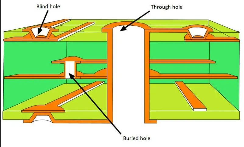
Vias are plated through-holes that provide vertical conduction paths in multilayer PCBs, allowing signals, power, and ground to transition between layers. In standard through-hole vias, the hole penetrates the entire board thickness, making them simple but consuming valuable surface area in dense layouts. Blind vias connect an outer layer to one or more inner layers without reaching the opposite side, while buried vias link only internal layers, invisible from the surfaces. These advanced via types support higher layer counts and finer pitch components by freeing up outer layers for routing. For electrical engineers, understanding these distinctions is critical because improper via selection can introduce impedance discontinuities or increase crosstalk in high-speed circuits. Ultimately, via choice influences manufacturability, cost, and electromagnetic compatibility in real-world applications.
The relevance of PCB via design grows with the demand for compact electronics in sectors like telecommunications and computing. Through vias suffice for low-density boards but limit routing in multilayer stacks exceeding eight layers. Blind and buried vias enable tighter interconnects, reducing board size by up to 30 percent in high-density interconnect designs. Microvias further push boundaries with their small dimensions, ideal for ball grid array packages. Neglecting via optimization can lead to signal degradation or thermal hotspots, compromising system reliability. Engineers prioritize via strategies early in the design phase to align with performance goals.
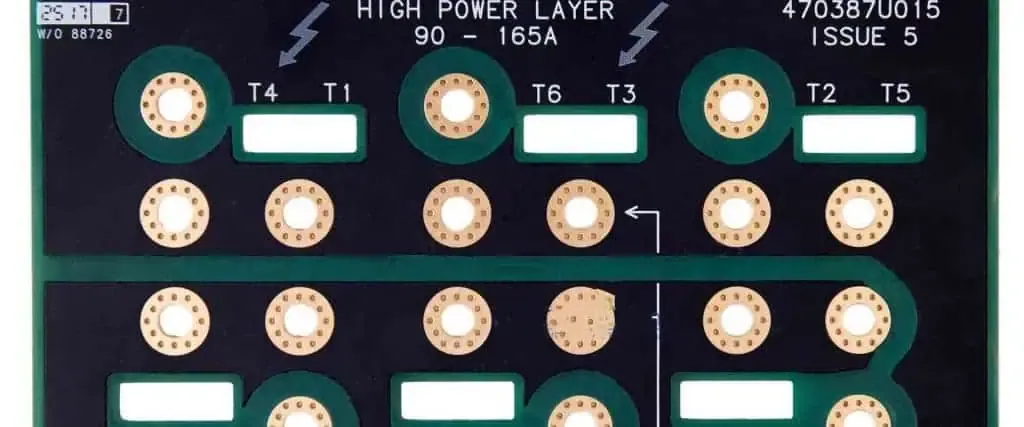
Different Via Styles in PCB Via Design
PCB via design encompasses several styles, each suited to specific routing needs and fabrication capabilities. Through-hole vias offer the simplest structure, drilled through all layers and plated for conduction, but they interrupt inner layer planes extensively. Blind vias start from one surface and end at an inner layer, preserving the opposite side for components or traces. Buried vias reside entirely within the stackup, connecting inner layers without surface access, which demands sequential lamination processes. Microvias, often laser-drilled, feature diameters under 150 micrometers and shallow depths, classified as stacked or staggered based on alignment.
Additional styles include via-in-pad, where the via lands directly under component pads for space savings, and tented vias, covered with solder mask to protect against contaminants. Stacked microvias align vertically across multiple layers for compact transitions, while staggered ones offset to ease plating. Each style trades off density against reliability; for instance, through vias excel in mechanical strength but falter in high-frequency applications due to stubs. Electrical engineers select styles based on stackup height, signal speed, and power demands. IPC-2221 provides guidelines on via integrity and spacing to ensure design consistency across these variations. Proper selection prevents issues like via breakout failures during assembly.
PCB Blind and Buried Vias: Design and Implementation
PCB blind and buried vias enhance multilayer efficiency by limiting drill depth and preserving routing space. Blind vias facilitate connections from layer 1 to layer 3, for example, without penetrating deeper, which reduces stub inductance in signal paths. Buried vias, formed between layers 2 and 4, avoid surface exposure entirely, ideal for power planes. Manufacturing involves sequential build-up: outer layers laminate first for blind vias, then inner cores add buried structures. This process increases cost but yields denser boards compliant with high-reliability standards. Engineers must specify layer pairs precisely in design files to guide fabricators.
Design considerations include annular ring dimensions and plating uniformity to withstand thermal cycling. IPC-6012 outlines acceptability criteria for these vias, emphasizing void-free barrels. Blind vias improve signal integrity by shortening return paths, while buried vias minimize electromagnetic interference between planes. In practice, combining both types optimizes 12-layer or higher stackups. Limitations arise from alignment tolerances during lamination, potentially causing open circuits if not controlled. Electrical engineers verify designs through cross-section analysis during prototyping.
Micro Via Manufacture: Processes and Challenges
Micro via manufacture targets high-density interconnects using precise drilling and filling techniques. Laser ablation creates holes smaller than mechanical drills can achieve, followed by electroless copper seeding and electroplating. The process adheres to a 1:1 aspect ratio maximum, as defined in IPC standards, to ensure reliable plating coverage. Stacked microvias build sequentially, with each level filled and planarized, while staggered avoid direct stacking to reduce stress. Challenges include resin smear removal via desmear and controlling dielectric thickness for uniform deposition.
Post-plating, vias often fill with conductive epoxy for planarity and thermal conductivity. Manufacturing yields drop with via counts exceeding thousands per square inch due to registration errors. Electrical engineers mitigate risks by limiting stack heights to any-layer interconnect class 2 or 3. Quality checks involve electrical testing and microscopy for plating thickness, typically targeting minimum averages per IPC-6012. Successful micro via integration demands collaboration between design and fabrication teams.
High Current Vias: Electrical and Thermal Management
High current vias carry substantial amperage between power planes, necessitating robust sizing and multiplicity. Single vias suffice for low currents but risk overheating; arrays or stitching vias distribute load effectively. Plating thickness, often 20 micrometers minimum per class 2/3 rules, supports conduction without excessive resistance. Electrical engineers calculate capacity considering barrel cross-section and temperature rise, paralleling multiple vias for redundancy. Thermal vias under power components enhance heat dissipation to inner planes.
Design best practices include larger diameters and filled vias to boost current handling. Stitching places vias in grids around high-power paths, providing low-impedance returns. Impedance mismatches arise if via inductance exceeds trace values, so model in simulations. JEDEC thermal standards guide via placement in test boards for power integrity validation. Overlooking these leads to electromigration or delamination under load. Optimized high current vias ensure long-term reliability in demanding environments.
Best Practices for PCB Via Design
Effective PCB via design follows structured rules for reliability and performance. Maintain aspect ratios below 10:1 for through vias to guarantee plating uniformity, adjusting drill sizes per stackup thickness. Annular rings should exceed minimums by 50 percent for breakout prevention during fabrication. Use blind or buried vias strategically to preserve outer layer real estate in dense areas. For signals, position vias near bends to minimize stubs, and tent non-critical ones for protection.
Simulate via impedance for high-speed lines, targeting 50 ohms single-ended matches. Array high current vias with 1-2 mm pitch, filling with conductive material for enhanced thermal paths. Incorporate IPC-2221 recommendations for via protection and spacing in multilayer stacks. Prototype with cross-sections to validate plating and fill. Document layer-specific via definitions clearly. These practices reduce iterations and align with manufacturability.
Troubleshooting Common Via Issues
Via failures manifest as opens, high resistance, or intermittent connections in multilayer PCBs. Plating voids stem from poor aspect ratios or contaminated holes, detectable via resistance mapping. Cracking occurs from thermal mismatch during reflow, especially in microvias with rigid fills. Engineers troubleshoot by sectioning suspect boards and inspecting under microscopy.
Barrel pull-away at layer interfaces signals adhesion issues, often from inadequate desmear. For high current vias, overheating indicates undersizing; measure temperature with IR imaging. Blind via misalignment causes incomplete connections, resolved by tightening drill registration. Systematic DFM reviews prevent recurrence. Cross-referencing against IPC-6012 acceptance criteria accelerates root cause analysis. Proactive design rules minimize field failures.
Conclusion
Mastering PCB via design unlocks the full potential of multilayer boards for electrical engineers. From basic through vias to advanced microvia arrays, each style addresses unique density and performance needs. Blind and buried vias optimize inner routing, while high current strategies ensure power integrity. Adhering to best practices like aspect control and simulation yields reliable outcomes. Micro via manufacture, though challenging, enables cutting-edge interconnects. Apply these insights to elevate your designs systematically.
FAQs
Q1: What are the main differences between blind and buried vias in PCB via design?
A1: Blind vias connect surface layers to inner ones without full penetration, saving outer space, while buried vias link only internal layers, invisible externally. Both require sequential lamination but buried types demand higher precision. They enhance density in multilayer PCBs over through vias. Use blind for signal transitions and buried for planes.
Q2: How does micro via manufacture impact high-density PCBs?
A2: Micro via manufacture uses laser drilling for small apertures, achieving 1:1 aspect ratios per IPC definitions. Challenges include plating uniformity and fill planarity. They enable finer pitches for BGA components. Electrical engineers benefit from increased routing channels in HDI boards.
Q3: What considerations apply to high current vias?
A3: High current vias need larger sizes, thicker plating, and arrays to distribute heat and resistance. Stitching improves thermal paths to planes. Model current density to avoid electromigration. Combine with wide traces for optimal performance.
Q4: When should electrical engineers choose different via styles?
A4: Through vias suit simple, low-density boards; blind and buried for multilayer density. Microvias fit HDI with fine-pitch needs. Factor stackup, speed, and current. IPC-2221 guides selection for integrity.
References
IPC-2221 — Generic Standard on Printed Board Design. IPC
IPC-6012E — Qualification and Performance Specification for Rigid Printed Boards. IPC, 2017
IPC-A-600K — Acceptability of Printed Boards. IPC, 2020