Introduction
Microvia stackup is a critical concept in modern printed circuit board (PCB) design, especially for electronic hobbyists venturing into high-density interconnect (HDI) projects. As devices shrink and functionality grows, understanding how to structure layers and vias becomes essential for compact, reliable designs. This guide aims to simplify microvia stackup, offering a clear path for beginners to grasp its principles and apply them in hobbyist projects. Whether you are designing a small IoT gadget or a complex prototype, mastering this technique ensures better signal integrity and space efficiency. We will explore the basics, technical aspects, and practical tips to help you navigate this advanced PCB topic with confidence. Let’s dive into why microvia stackup matters and how it can elevate your electronic creations.
What Is Microvia Stackup and Why It Matters
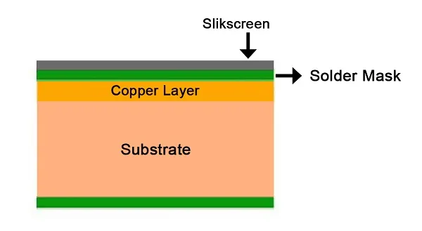
Microvia stackup refers to the arrangement of layers and microvias in a multilayer PCB to enable high-density connections between components. Microvias are tiny vias, typically less than 0.15 millimeters in diameter, drilled using laser technology to connect adjacent layers. Unlike traditional through-hole vias, they save space and support finer traces, making them ideal for compact designs. In a stackup, these microvias are strategically placed to form connections without occupying excessive board area.
For electronic hobbyists, microvia stackup is vital when working on projects with limited space, such as wearable devices or miniature sensors. It allows more components to fit on smaller boards while maintaining electrical performance. Proper stackup design also reduces signal interference and improves reliability. Ignoring these principles can lead to manufacturing issues or poor functionality, impacting project success. Understanding this concept opens doors to advanced PCB layouts that meet modern demands.
Related Reading: Microvia Design for EMI Reduction
Technical Principles of Microvia Stackup
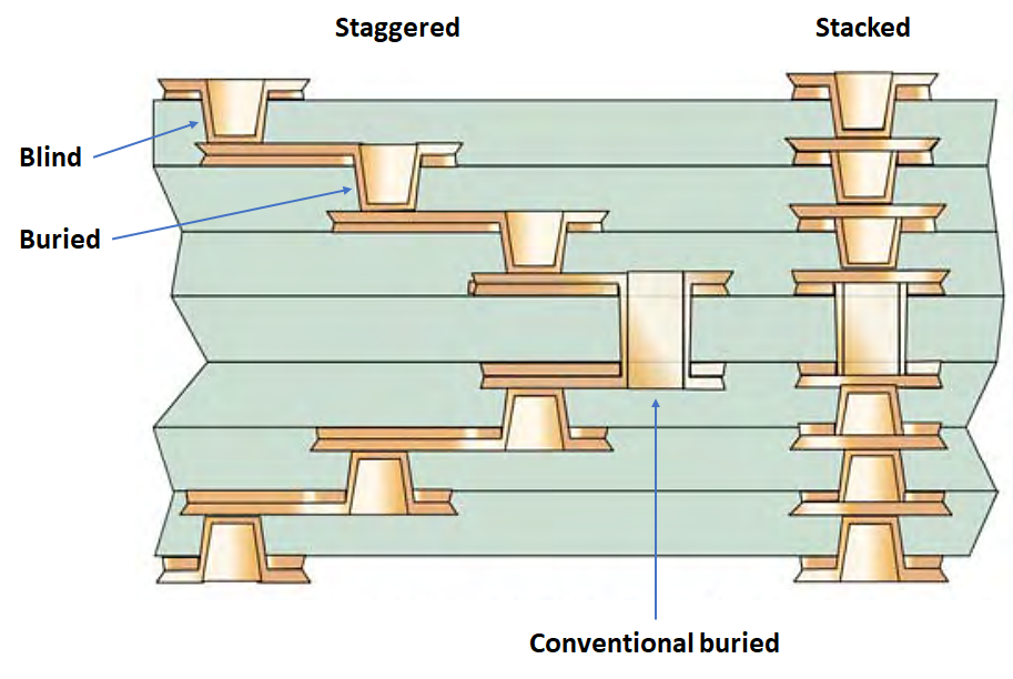
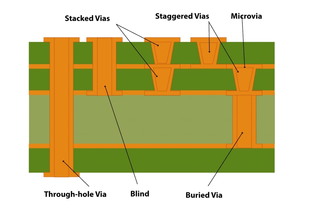
Microvias are fundamental to HDI designs, and their placement within a stackup follows specific engineering principles. A stackup defines the sequence of conductive and insulating layers in a PCB, along with the vias connecting them. Microvias are often used in a staggered or stacked configuration. Staggered microvias connect layers with slight offsets, while stacked microvias align directly on top of each other for deeper connections.
The aspect ratio, or the ratio of via depth to diameter, is a key consideration. Industry guidelines, such as those outlined in IPC-2226, recommend keeping this ratio low, typically below 1:1, to ensure manufacturability and reliability. A higher ratio risks incomplete drilling or structural weakness. Additionally, microvias are usually laser-drilled, allowing precision in small diameters, unlike mechanical drilling used for larger vias.
Layer pairing is another principle. Microvias typically connect only adjacent layers, reducing complexity. For instance, in a six-layer board, a microvia might link layer one to layer two, while another connects layer two to layer three. This approach minimizes signal path length, enhancing performance. Adhering to standards like IPC-T-50M for terminology and design ensures consistency in understanding these structures.
Thermal and electrical properties also influence stackup design. Dielectric materials between layers must handle heat dissipation and maintain signal integrity. Selecting materials compatible with laser drilling, as suggested by industry best practices, prevents issues during fabrication. For hobbyists, recognizing these principles helps avoid common pitfalls in multilayer designs.
Best Practices for Designing Microvia Stackup
Creating a reliable microvia stackup as a hobbyist requires attention to detail and adherence to proven practices. Start by defining the number of layers needed for your project. A four or six-layer board is often sufficient for most compact designs. Plan the stackup symmetry to balance copper distribution, reducing the risk of board warpage during manufacturing.
Follow industry guidelines for microvia placement. According to IPC-2226, microvias should connect only adjacent layers to maintain structural integrity. Avoid stacking more than two microvias directly, as this increases fabrication complexity and potential failure points. If deeper connections are needed, use staggered configurations to distribute stress evenly across layers.
Choose appropriate dielectric materials. Opt for materials with consistent thickness and laser-drillable properties to ensure clean microvia formation. Consult material datasheets for compatibility with HDI processes, keeping thermal expansion in mind to prevent delamination. For hobbyists, starting with standard FR-4 material can be a cost-effective choice for learning.
Pay attention to trace routing. Keep signal traces short and direct when using microvias to minimize impedance mismatches. Place ground planes near signal layers to reduce electromagnetic interference. Simulation tools, widely available for free or at low cost, can help visualize signal behavior before finalizing the design.
Finally, verify your design against manufacturing capabilities. Many fabrication houses specify minimum microvia sizes and aspect ratios in their design rules. Ensure your stackup aligns with these constraints to avoid production delays. Document every layer and connection clearly in your design files to prevent miscommunication during fabrication.
Related Reading: Microvia PCB Design Rules: A Practical Handbook for Error Free HDI Layouts
Common Challenges and Troubleshooting Tips
Electronic hobbyists often face hurdles when incorporating microvia stackup in their PCB designs. One frequent issue is misalignment during layer stacking, leading to unreliable connections. To address this, double-check layer registration in your design files before submission. Use alignment markers on each layer to assist manufacturers in maintaining precision.
Another challenge is microvia failure due to thermal stress. Repeated heating and cooling cycles can cause cracks if materials are mismatched. Select dielectric layers with similar coefficients of thermal expansion to minimize stress. Following guidelines in IPC-6012E for material performance can help prevent such issues.
Signal integrity problems may arise from improper stackup planning. Long signal paths through multiple microvias can introduce noise. Keep critical signals on outer layers whenever possible, using microvias only for necessary interlayer connections. Adding reference planes, as recommended by industry practices, stabilizes signal return paths.
Manufacturing limitations can also pose difficulties. Some hobbyist-friendly fabrication services may not support advanced HDI features like stacked microvias. Research service capabilities upfront and adjust your design to match their constraints. If errors occur, review fabrication feedback to identify stackup design flaws for correction in future iterations.
Conclusion
Microvia stackup is a powerful tool for electronic hobbyists aiming to create compact, high-performance PCBs. By understanding its principles, such as layer arrangement and microvia placement, you can design boards that meet modern density requirements. Applying best practices, like adhering to industry standards and selecting suitable materials, ensures reliability and manufacturability. While challenges like thermal stress or signal issues may arise, practical troubleshooting tips can guide you through solutions. Mastering this aspect of PCB design empowers you to push the boundaries of your projects, achieving professional results even as a beginner. With this guide, you are equipped to explore microvia stackup confidently in your next creation.
FAQs
Q1: What is a microvia stackup, and why should hobbyists care about it?
A1: A microvia stackup refers to the layered arrangement of a PCB with tiny microvias connecting adjacent layers for high-density designs. Hobbyists should care because it enables compact layouts for small projects like wearables or IoT devices. It saves space, improves signal performance, and supports complex circuits in limited areas, making it a valuable skill for modern electronics tinkering.
Q2: How do I start designing a microvia stackup for my first PCB project?
A2: Begin by determining the number of layers your project needs, typically four or six for beginners. Plan microvia connections between adjacent layers only, following guidelines like IPC-2226. Use free or low-cost design software to map out layers and vias. Check manufacturer design rules to ensure compatibility, and document every detail clearly for fabrication success.
Q3: What are common mistakes in microvia stackup design for beginners?
A3: Beginners often overlook layer symmetry, leading to warpage, or stack too many microvias, risking failure. Ignoring material compatibility for laser drilling can cause fabrication issues. Not verifying manufacturer capabilities is another error. Always balance copper distribution, limit stacked microvias, choose suitable materials, and confirm service constraints to avoid costly redesigns.
Q4: How can I ensure reliability in my microvia stackup design?
A4: Ensure reliability by keeping microvia aspect ratios low, as per IPC-2226 recommendations, to avoid structural weakness. Use materials with matching thermal properties to prevent stress cracks. Place ground planes near signal layers for interference reduction. Review your design against industry standards like IPC-6012E, and test simulations if possible before finalizing the layout.
IPC-2226 — Design Standard for High Density Interconnect (HDI) Printed Boards. IPC, 2003.
IPC-T-50M — Terms and Definitions for Interconnecting and Packaging Electronic Circuits. IPC, 2015.
IPC-6012E — Qualification and Performance Specification for Rigid Printed Boards. IPC, 2020.