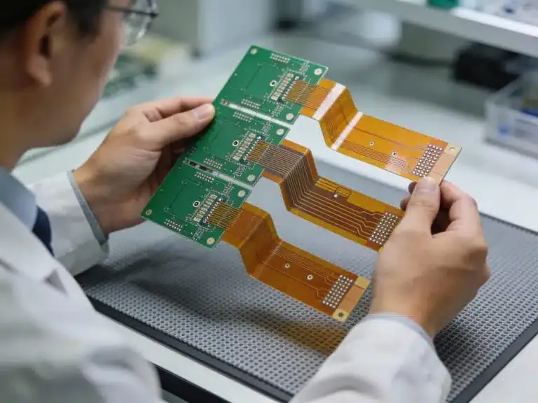
Introduction
In high-density interconnect (HDI) PCB design, microvias play a pivotal role in achieving compact layouts with superior routing density. The pcb microvia drill size directly influences electrical performance, thermal management, and manufacturing yield. Engineers must balance the push for smaller diameters to maximize board space against reliability constraints imposed by plating quality and mechanical stress. Laser drilling microvias has become the standard method to produce these fine features, enabling diameters well below traditional mechanical limits. This article explores the minimum achievable drill sizes, key design parameters like microvia aspect ratio, and strategies for implementing stacked microvias in HDI pcb design. Understanding these elements ensures robust designs that meet stringent performance requirements.
Defining Microvias and Their Role in HDI PCBs
Microvias are small blind or buried vias characterized by their limited size and depth, typically used to connect adjacent layers in multilayer boards. Industry definitions classify a microvia as any hole with a diameter of 150 micrometers or less, distinguishing it from standard vias drilled mechanically. This size threshold supports the high interconnection density essential for modern electronics like smartphones and medical devices. The pcb microvia drill size determines the minimum land size and trace spacing, directly impacting overall board miniaturization. In HDI pcb design, microvias replace larger through-holes, freeing up surface area for components. Their shallow depth, often no more than 0.25 millimeters, aligns with the need for precise layer-to-layer transitions without penetrating the entire stackup.
The relevance of minimum drill sizes stems from the exponential growth in component pin counts and I/O densities. Smaller microvia drills allow engineers to route more signals in congested areas, improving signal integrity by shortening paths. However, pushing diameters too small risks incomplete plating or void formation during fabrication. Laser drilling microvias addresses these challenges by providing sub-100 micrometer precision unattainable with mechanical methods. Designers must consider material compatibility, as resin types affect ablation rates and hole taper. Ultimately, selecting the appropriate minimum size optimizes both density and manufacturability.
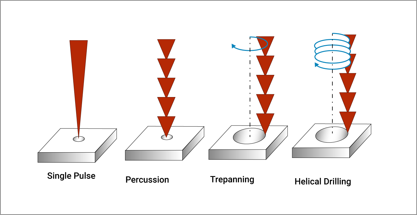
Laser Drilling Microvias: Principles and Capabilities
Laser drilling microvias relies on ablative processes where a focused beam vaporizes dielectric material to form the hole. Ultraviolet (UV) lasers excel at drilling through copper and resin composites, producing straight-sided holes with minimal heat-affected zones. Carbon dioxide (CO2) lasers suit thicker dielectrics but may introduce conical profiles due to longer wavelengths. The pcb microvia drill size achievable depends on laser pulse duration, repetition rate, and power density, often reaching 50 to 75 micrometers in production environments. Post-drill desmear removes residue, ensuring clean walls for electroless copper plating. This sequence enables reliable conduction paths in high-volume manufacturing.
Key limitations arise from beam spot size and material absorption, setting practical floors for minimum diameters. For instance, advanced systems achieve 40 micrometers experimentally, but standard HDI processes favor 75 to 100 micrometers for yield stability. Hole entrance and exit diameters must maintain uniformity to avoid plating discontinuities. Engineers evaluate drill quality via cross-section analysis, checking for sidewall roughness below specified limits. Integrating these techniques into HDI pcb design requires simulation tools to predict thermal gradients during drilling. Consistent process control minimizes variations across panels.
Microvia Aspect Ratio: A Critical Design Parameter
The microvia aspect ratio, defined as the ratio of hole depth to diameter, governs plating uniformity and electromigration resistance. Industry guidelines recommend a maximum of 1:1, with optimal values around 0.75:1 to 0.8:1 for robust copper deposition. Exceeding this leads to pinched-off tops or bottom voids, compromising via reliability under thermal cycling. In HDI pcb design, thinner core dielectrics, typically 50 to 100 micrometers, pair with small pcb microvia drill sizes to maintain favorable ratios. Depth control during laser drilling is paramount, as over-drilling erodes target pads. Designers calculate aspect ratio early in stackup planning to align with fabrication capabilities.
Plating chemistry further influences tolerable ratios, with pulse reverse electroplating mitigating buildup at hole entrances. Reliability testing validates designs at elevated ratios, simulating field conditions like temperature swings. IPC-6012DS outlines performance requirements for microvias, including minimum plating thickness in blind structures. Adhering to these ensures vias withstand mechanical stress without cracking. Aspect ratio also affects capacitance, making it a signal integrity factor in high-speed designs. Balancing it with drill size unlocks denser interconnects.
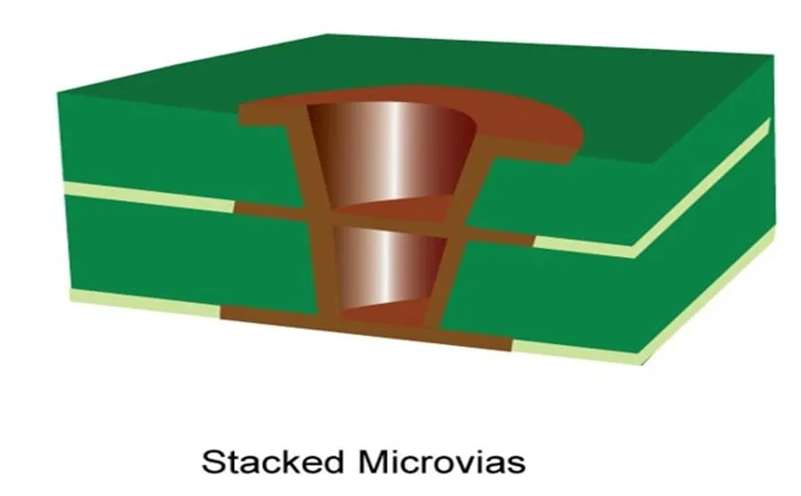
Stacked Microvias: Rules and Reliability Considerations
Stacked microvias involve multiple blind vias aligned vertically, spanning more than one layer pair for extended reach. This configuration amplifies density but concentrates stress at interfaces, demanding strict design rules. Maximum stacks are typically limited to two or three vias to mitigate fatigue failure, with staggered arrangements distributing loads better than pure stacks. The pcb microvia drill size in stacks must align precisely, often requiring 10 micrometer tolerances for pad capture. Laser drilling microvias sequentially builds these structures, with intermediate plating filling lower levels. HDI pcb design stackups classify boards by microvia types, such as Type III for 2+n+2 configurations.
Reliability hinges on via fill methods: electroplated copper outperforms conductive pastes in thermal conductivity. IPC-2226 provides guidelines for HDI interconnects, emphasizing capture and target land dimensions relative to drill size. Stacking increases warpage risk during lamination, necessitating symmetric builds. Engineers model thermomechanical behavior to predict crack propagation sites. Via-in-pad designs integrate stacked microvias seamlessly, reducing stub inductance. Proper implementation yields boards with escape routing for fine-pitch BGAs exceeding 0.5 millimeters.
Best Practices for Minimum Drill Size in HDI Design
Start with stackup optimization, selecting low-CTE dielectrics to match microvia dimensions and minimize drill breakout. Define pcb microvia drill sizes conservatively, targeting 75 micrometers for Class 3 applications unless process data justifies smaller. Simulate plating throw using finite element models to verify aspect ratio compliance. Incorporate dog-bone or teardrop pads to enhance mechanical strength around small drills. For laser drilling microvias, specify beam parameters in fabrication notes, including fluence and overlap. Validate prototypes with electrical testing and thermal cycling per IPC standards.
Address signal integrity by fanning out microvias from BGA lands with minimal stubs. In stacked microvias, alternate drill sizes slightly to improve alignment yield. Monitor microvia aspect ratio across layers, adjusting dielectric thickness accordingly. Collaborate with fabricators early to confirm minimum achievable sizes based on equipment. Use design rule checks for annular ring adequacy, ensuring at least 50 micrometers external to the drill. These practices elevate HDI pcb design from feasible to field-proven.
Troubleshooting Common Microvia Challenges
Designers often encounter via opens traced to inadequate desmear, leaving carbon residue that blocks plating. Cross-sections reveal tapered holes from improper laser focus, inflating effective aspect ratios. In stacked microvias, misalignment causes target pad shorts, resolvable by fiducial marks and optical registration. Thermal cracking emerges in high-ratio designs post-reflow, mitigated by filled vias or epoxy plugs. Excessive drill sizes compromise density targets, while undersized ones fail yield specs. Systematic failure analysis, including dye-and-peel, pinpoints root causes like drill wander.
Conclusion
Mastering minimum pcb microvia drill size unlocks the full potential of HDI pcb design, enabling unprecedented density without sacrificing reliability. Laser drilling microvias, constrained by microvia aspect ratio and stack rules, demands precise engineering from concept to fabrication. Adhering to guidelines like those in IPC-6012DS and IPC-2226 ensures designs perform under real-world stresses. Engineers should prioritize simulation, process validation, and conservative sizing for optimal outcomes. As component densities rise, these techniques will define next-generation electronics.
FAQs
Q1: What is the typical minimum pcb microvia drill size in HDI designs?
A1: Laser drilling microvias enables diameters as small as 50 to 75 micrometers in advanced processes, though 75 to 100 micrometers is standard for reliable plating and yield. Factors like material and equipment set practical limits, with IPC guidelines classifying microvias at 150 micrometers or less. Designers select sizes balancing density and manufacturability in HDI pcb design.
Q2: How does microvia aspect ratio impact HDI pcb design?
A2: Microvia aspect ratio, ideally 0.75:1 to 1:1, ensures uniform plating and withstands thermal stress. Higher ratios risk voids or cracks, limiting stack heights. In HDI pcb design, it dictates dielectric thickness relative to pcb microvia drill size, influencing signal integrity and reliability.
Q3: What are the rules for stacked microvias?
A3: Stacked microvias are capped at two layers typically, with staggered preferred for stress distribution. Precise alignment of drill sizes prevents failures, per HDI guidelines. Laser drilling microvias builds them sequentially, requiring filled lower vias for stability in dense layouts.
Q4: Why use laser drilling for microvias?
A4: Laser drilling microvias achieves sub-150 micrometer precision unattainable mechanically, with controlled depth for blind structures. It supports small pcb microvia drill sizes and favorable aspect ratios in HDI pcb design. UV lasers minimize taper, ensuring plating quality essential for high-reliability boards.
References
IPC-6012DS — Qualification and Performance Specification for High Density Interconnect (HDI) Printed Boards. IPC, 2015
IPC-2226 — Design Standard for High Density Interconnects. IPC, 2001
IPC-6012E — Qualification and Performance Specification for Rigid Printed Boards. IPC, 2017