Introduction
Mixed-signal printed circuit boards integrate both analog and digital circuitry on the same board, creating unique challenges in routing that demand careful planning to maintain signal integrity. Electrical engineers face issues like noise coupling from fast-switching digital signals into sensitive analog paths, which can degrade performance in applications such as data acquisition systems and communication devices. Effective mixed-signal PCB routing strategies focus on separating signal types, controlling impedance, and minimizing interference to ensure reliable operation. These approaches not only reduce crosstalk but also optimize overall board performance by preserving signal fidelity across frequencies. As designs grow more complex with higher speeds and densities, mastering these routing techniques becomes essential for achieving robust electrical characteristics. This article explores proven methods for routing analog and digital signals while adhering to established engineering principles.
Understanding Mixed-Signal PCB Routing Challenges
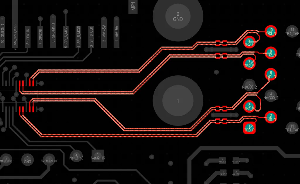
Mixed-signal PCB routing involves managing traces that carry both low-level analog signals and high-speed digital signals on shared layers or boards. Analog signals are particularly susceptible to interference from digital switching noise, which generates electromagnetic fields that couple into nearby conductors. Key challenges include crosstalk, where unwanted energy transfers between traces, and ground bounce caused by simultaneous switching of multiple digital outputs. Return path disruptions further exacerbate these problems, leading to signal distortion and reduced dynamic range in analog sections. Engineers must consider these interactions early in the design process to avoid costly respins. Industry guidelines, such as those in IPC-2221C, provide foundational rules for trace spacing and layer usage to mitigate such risks in mixed-signal environments.
The relevance of these challenges intensifies in high-performance applications where signal-to-noise ratios directly impact functionality. For instance, in sensor interfaces, even minor crosstalk can mask critical data, while in RF mixed-signal boards, poor routing amplifies harmonic distortion. Physical board constraints, like limited layer count, force compromises that heighten interference risks if not addressed systematically. Understanding these dynamics allows engineers to prioritize partitioning and controlled routing from the outset. Proper management ensures compliance with performance specifications and enhances manufacturability.
Key Technical Principles Behind Interference in Mixed-Signal PCBs
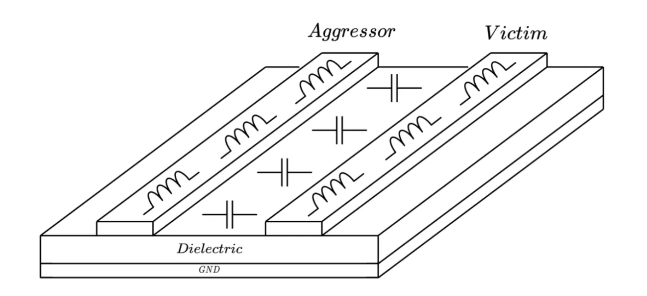
Crosstalk in PCB routing arises primarily from capacitive and inductive coupling between adjacent traces. Capacitive crosstalk occurs when electric fields between parallel traces induce voltage spikes on victim lines, proportional to the coupling capacitance and dv/dt of the aggressor signal. Inductive crosstalk, meanwhile, results from mutual inductance causing current-induced voltage on nearby conductors, especially pronounced in high-speed digital lines. Minimizing crosstalk in PCB routing requires increasing trace separation or using shielding to reduce field overlap. These principles guide the layout decisions that preserve signal quality in mixed-signal designs.
Impedance mismatch represents another critical factor, as uncontrolled variations lead to reflections that corrupt waveforms. Characteristic impedance depends on trace width, thickness, dielectric height, and material properties, necessitating precise stackup definitions. Differential pair routing in mixed-signal PCBs leverages balanced signaling to reject common-mode noise, but requires symmetric routing to maintain integrity. Ground planes provide low-impedance return paths, yet splitting them for analog and digital sections demands careful stitching to avoid slots that disrupt currents. These mechanisms underscore the need for simulation and verification during design.
Return path integrity ties all these elements together, as digital signals seek the shortest path back to the source through ground planes. In mixed-signal boards, analog sections benefit from dedicated planes to isolate clean references from noisy digital returns. Violations here amplify noise, emphasizing layered approaches over single-plane solutions.
Practical Best Practices for Mixed-Signal PCB Routing
Start with board partitioning to physically separate analog and digital sections, routing signals within their domains to limit crossovers. Place analog components near connectors or edges, away from digital ICs, and use moats or guard rings around sensitive areas. This strategy reduces field coupling and simplifies controlled impedance routing for mixed-signal applications. Maintain at least three times the dielectric height between partitioned sections, as recommended in design standards. Visual barriers like silkscreen lines aid fabrication awareness without affecting electrical performance.
Layer stackup planning is foundational, dedicating inner layers for analog signals over solid ground planes while reserving outer layers for digital routing. A typical 4-layer stack might feature signal-ground-signal-power, with analog on layers 2-3 and digital on 1 and 4. This configuration shields analog traces and provides reference planes for impedance control. For higher densities, 6-8 layers allow dedicated analog/digital planes, minimizing via transitions that introduce discontinuities. Adhering to IPC-2141A guidelines ensures impedance tolerances stay within 10% for high-speed lines.
When routing analog and digital signals, follow orthogonal rules: keep digital traces perpendicular to analog where crossings are unavoidable, and use ground vias as shields at intersections. Analog traces should be wider for lower resistance and routed first to secure clean paths, avoiding bends sharper than 3:1 ratios that increase radiation. Digital high-speed lines benefit from length-matched routing over continuous planes. These practices directly address minimizing crosstalk in PCB routing by controlling coupling coefficients.
Differential pair routing in mixed-signal PCBs demands intra-pair spacing of 5-10 mils and edge-to-edge separation from other signals exceeding 3 times the pair width. Length matching within 5 mils per inch of run compensates for skew, while constant spacing preserves differential impedance, often 90-100 ohms. Route pairs as coupled microstrips or striplines, avoiding vias mid-pair when possible. In mixed-signal contexts, position pairs away from analog clocks to prevent common-mode conversion.
Controlled impedance routing for mixed-signal requires field solver verification against stackup parameters, targeting single-ended 50 ohms and differential 100 ohms typical values. Adjust trace widths accordingly, factoring in etch tolerances of ±10%. Fabricate test coupons on panels for TDR validation post-production. IPC-6012F performance specs validate these efforts through electrical testing.
Incorporate guard traces or stitching vias along analog boundaries to shunt noise to ground. Power distribution uses decoupled planes with ferrites at boundaries. These layered defenses maximize performance while simplifying debugging.
Troubleshooting Common Routing Issues in Mixed-Signal Designs
Engineers often detect poor mixed-signal PCB routing through oscilloscope probing revealing noise spurs or eye diagram closure. Crosstalk manifests as glitches on analog outputs synchronous with digital edges, traceable to parallel runs. Use spectrum analysis to quantify coupling levels exceeding -60 dB targets. Ground bounce appears as baseline shifts during bursts, fixed by adding decoupling closer to ICs.
Reflections from impedance steps cause ringing, confirmed via TDR plots. Shorten stubs, add series termination, or reroute for continuity. Partition failures show broadband noise floors elevated by 10-20 dB; widen moats or add shielding. Systematic post-layout simulation catches 80% of issues before fab.
Conclusion
Mastering mixed-signal PCB routing hinges on partitioning, impedance control, and disciplined trace management to minimize interference. By separating analog and digital domains, employing differential techniques, and leveraging ground planes, engineers achieve superior signal integrity. Standards like IPC-2221C, IPC-2141A, and IPC-6012F provide the framework for reliable designs. Implementing these strategies ensures high performance in demanding applications, reducing risks and iterations. Prioritize early planning and verification for optimal results.
FAQs
Q1: What is mixed-signal PCB routing, and why is it challenging?
A1: Mixed-signal PCB routing involves laying out traces for both analog and digital signals on the same board. Challenges arise from digital noise coupling into analog paths via crosstalk and EMI, degrading SNR. Partitioning and orthogonal routing mitigate these, ensuring clean analog performance alongside digital speed. Follow design guidelines for spacing to maintain integrity.
Q2: How do you perform differential pair routing in mixed-signal PCBs?
A2: Differential pair routing requires symmetric traces with fixed spacing and length matching to preserve balance. Route over solid reference planes, keeping pairs isolated from single-ended analog lines. Target 100-ohm impedance with 5-mil matching tolerance. This rejects common-mode noise effectively in mixed environments.
Q3: What are effective ways of minimizing crosstalk in PCB routing?
A3: Minimize crosstalk by increasing trace separation, using ground planes underneath, and routing signals orthogonally. Shield with guard traces or vias at crossings. Control rise times and lengths for high-speed lines. These steps reduce coupling below -50 dB in mixed-signal designs.
Q4: Why is controlled impedance routing critical for mixed-signal PCBs?
A4: Controlled impedance prevents reflections that distort signals, vital for high-speed digital and precise analog. Calculate trace geometries per stackup to hit targets like 50 ohms single-ended. Verify with coupons to ensure tolerance, enhancing overall performance.
References
IPC-2221C — Generic Standard on Printed Board Design. IPC, 2023
IPC-2141A — Design Guide for High-Speed Controlled Impedance Interconnects. IPC, 2017
IPC-6012F — Qualification and Performance Specification for Rigid Printed Boards. IPC, 2023