Introduction
Mixed-signal printed circuit boards integrate analog and digital circuits, creating unique challenges in maintaining signal quality amid high-speed operations. Electromagnetic interference from digital switching can couple into sensitive analog paths, degrading performance in applications like data acquisition systems and sensor interfaces. Proper mixed-signal PCB stack-up design addresses these issues by strategically arranging layers to enhance EMI shielding in PCB stack-up and preserve signal integrity considerations for PCB stack-up. Engineers must balance layer count, material properties, and routing strategies to achieve reliable operation. This approach not only minimizes crosstalk but also supports controlled impedance for both signal types. Understanding these fundamentals allows for robust designs that meet demanding electrical requirements.
What Is a Mixed-Signal PCB Stack-Up and Why It Matters
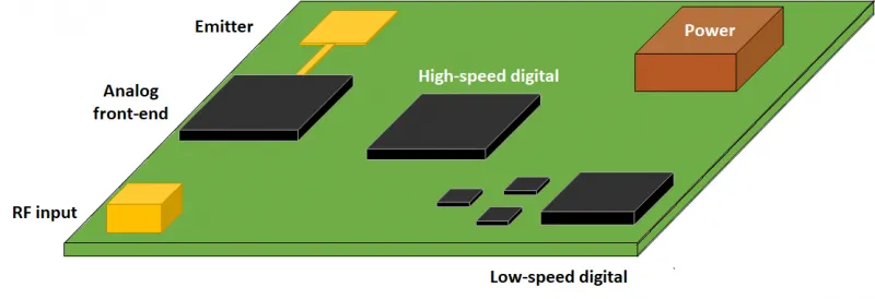
A mixed-signal PCB stack-up refers to the vertical arrangement of conductive layers, dielectrics, and planes in a multilayer board tailored for combined analog and digital functions. Each layer serves specific roles, such as signal routing, power distribution, or grounding, with precise thicknesses defining electrical characteristics. In contrast to pure digital or analog boards, the PCB layer stack for mixed-signal demands partitioned sections to isolate noisy digital environments from precision analog areas. This configuration directly influences parasitic capacitance, inductance, and coupling between layers.
The importance of optimizing PCB stack-up for analog and digital circuits stems from the inherent noise generation in digital transitions, which produce broadband EMI that radiates or conducts into analog circuits. Poor stack-up leads to signal distortion, increased bit error rates, and compliance failures in regulated environments. Conversely, a well-planned stack-up provides shielding, low-impedance return paths, and impedance matching, ensuring signals propagate with minimal degradation. For electrical engineers, mastering this aspect reduces iterations during prototyping and enhances overall board reliability. Industry demands for higher integration densities amplify these needs, making stack-up a foundational design decision.
Key Technical Principles Governing EMI and Signal Integrity
Electromagnetic interference in mixed-signal designs arises primarily from fast digital edges creating displacement currents and radiating fields that couple through dielectrics or apertures. Ground planes act as shields by providing low-impedance paths for return currents, confining fields between layers and reducing radiated emissions. Signal integrity considerations for PCB stack-up involve maintaining characteristic impedance, typically 50 ohms for single-ended or 100 ohms for differential lines, through consistent dielectric height and width-to-height ratios. Variations in stack-up symmetry can introduce mode conversion or reflections at vias, exacerbating issues.
Plane capacitance between power and ground layers forms distributed decoupling, stabilizing voltage rails and filtering high-frequency noise before it affects analog sections. In mixed-signal contexts, separate analog and digital ground planes prevent digital ground bounce from modulating analog references, with connection at a single low-inductance point. Dielectric materials with low loss tangents minimize attenuation for analog signals, while thinner cores enable tighter coupling for digital high-speed lines. These principles align with established guidelines that emphasize continuous planes and adjacent reference layers for optimal field containment.
Thermal expansion mismatches across layers can warp boards, altering clearances and introducing mechanical stress on traces, indirectly impacting EMI through deformed apertures. Adhering to IPC-2221B for layer spacing and plane design helps mitigate such risks by promoting symmetric builds. Engineers evaluate stack-up via field solvers to quantify coupling coefficients and insertion loss, ensuring margins against worst-case scenarios.
Best Practices for Optimizing Mixed-Signal PCB Stack-Ups
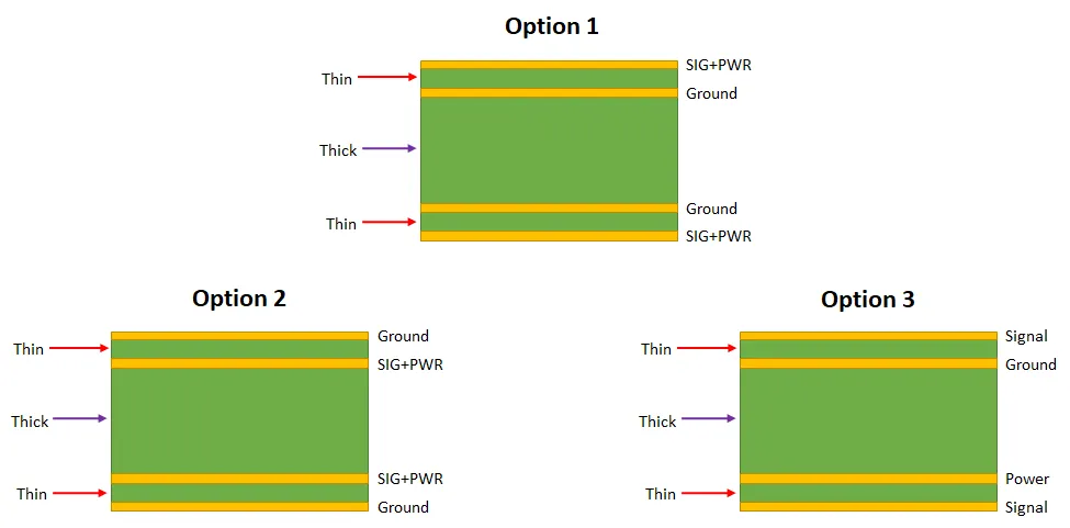
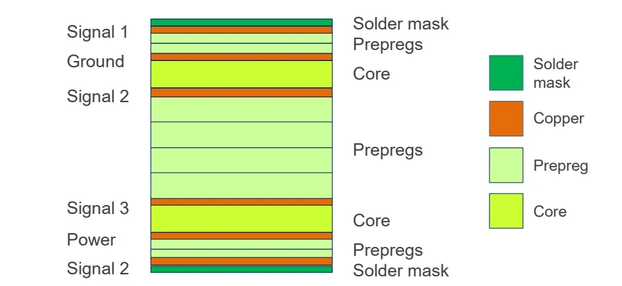
Start with a minimum of four layers for basic mixed-signal boards, arranging as top signal (digital), full ground, power plane, and bottom signal (analog). This setup sandwiches signals between planes, providing dual-sided shielding and short return paths. For higher densities, six-layer configurations offer dedicated analog and digital routing layers: Layer 1 (digital signals), Layer 2 (digital ground), Layer 3 (power), Layer 4 (analog ground), Layer 5 (analog signals), Layer 6 (mixed signals or ground). Maintain dielectric thicknesses around 0.1 to 0.2 mm between signal and plane for strong coupling, adjusting for impedance targets.
Implement EMI shielding in PCB stack-up by stitching ground vias along partition boundaries, creating Faraday cage-like enclosures without splitting planes excessively. Segment power planes to match circuit domains, using decoupling capacitors at splits to block noise propagation. Route sensitive analog traces as inner microstrips adjacent to analog ground, avoiding proximity to digital vias that act as antennas. Differential pairs benefit from symmetric stack-up to preserve balance and minimize common-mode noise pickup.
- 4-Layer — Sig (Digital), GND, PWR, Sig (Analog): Cost-effective shielding, basic impedance control
- 6-Layer — Sig (Dig), DGND, PWR, AGND, Sig (Ana), GND: Isolated grounds, enhanced decoupling
- 8-Layer — Sig (Dig), DGND, Sig (Dig), PWR, PWR, AGND, Sig (Ana), GND: High-speed routing with dual references
Use this list as a starting point, simulating each for specific frequencies. Symmetry in core and prepreg thicknesses prevents warpage per IPC-6012E performance specs, preserving layer alignments over temperature cycles. Blind or buried vias reduce stub lengths, improving high-frequency SI.
For power integrity, interleave power and ground planes to maximize capacitance, calculated as εA/d where ε is permittivity, A area, d separation. Avoid routing clock lines on outer layers; bury them between planes to contain emissions. Finalize stack-up with manufacturer input on achievable tolerances, iterating based on impedance profiles.
Troubleshooting Common Stack-Up Issues in Mixed-Signal Designs
Ground loops often emerge when analog and digital grounds connect through multiple paths, injecting noise via shared impedance. Diagnose by probing voltage differentials across partitions and mitigate with a star-point connection under the ADC or interface IC. Crosstalk spikes in simulations indicate inadequate plane proximity; thicken dielectrics selectively or add shield layers. If SI eye diagrams close prematurely, check via transitions for resonance, applying back-drilling where feasible.
Warpage from asymmetric builds alters trace lengths, causing phase skew in clocks. Measure flatness post-reflow and redesign for balance if exceeding limits. High EMI emissions at board edges suggest incomplete shielding; extend ground pours and add edge vias. These fixes, grounded in systematic verification, resolve most issues without respins.
Conclusion
Effective mixed-signal PCB stack-up design hinges on principled layer planning that prioritizes EMI shielding and signal integrity. By dedicating reference planes, partitioning domains, and enforcing symmetry, engineers create resilient boards for integrated circuits. Practical adherence to configurations like six-layer isolated grounds yields measurable improvements in noise margins and compliance. Continuous evaluation through modeling refines these choices, ensuring performance in evolving high-density applications. Mastering these elements elevates design efficiency and reliability.
FAQs
Q1: What is the ideal PCB layer stack for mixed-signal designs?
A1: The ideal PCB layer stack for mixed-signal prioritizes ground planes adjacent to signal layers, such as a 6-layer setup with digital signals over digital ground, followed by power, analog ground, analog signals, and a full ground. This arrangement optimizes PCB stack-up for analog and digital circuits by minimizing loop areas and providing shielding. Maintain thin dielectrics between signals and planes for impedance control around 50 ohms. Simulate to verify before fabrication.
Q2: How does EMI shielding in PCB stack-up improve mixed-signal performance?
A2: EMI shielding in PCB stack-up confines digital noise through continuous ground planes and via fences, preventing coupling to analog traces. Place sensitive nets between dual references to attenuate fields by over 20 dB typically. Segment planes judiciously to avoid slots that radiate. This practice upholds signal integrity considerations for PCB stack-up, reducing spurs in FFT spectra of analog outputs.
Q3: What are key signal integrity considerations for PCB stack-up in mixed-signal boards?
A3: Signal integrity considerations for PCB stack-up include consistent dielectric heights for impedance matching, symmetric builds to avoid warpage-induced skew, and buried routing for high-speed lines. Dedicate inner layers for critical nets with nearby planes to shorten return paths. Account for via parasitics in transitions. These ensure clean eye patterns and low jitter across frequencies.
Q4: Why separate analog and digital grounds in a mixed-signal PCB stack-up?
A4: Separating analog and digital grounds in a mixed-signal PCB stack-up prevents digital switching noise from contaminating analog references via shared bounce. Connect them at one point near the interface to equalize potentials without loops. This enhances EMI shielding in PCB stack-up and preserves dynamic range. Monitor with scopes during layout reviews.
References
IPC-2221B — Generic Standard on Printed Board Design. IPC, 2003
IPC-6012E — Qualification and Performance Specification for Rigid Printed Boards. IPC, 2017
IPC-A-600K — Acceptability of Printed Boards. IPC, 2020