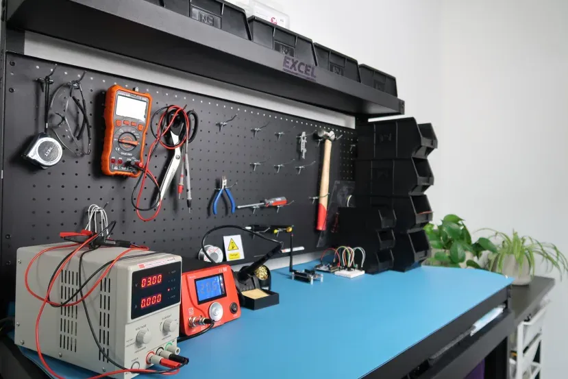
Introduction
Mobile phone PCBs demand precision assembly to pack high-density components into compact spaces while ensuring reliability under thermal and mechanical stress. The SMT assembly process dominates this field, enabling automated production at scale with minimal defects. Reflow soldering PCB stands as the core step, melting solder paste to form durable joints without manual intervention. Engineers must grasp these processes to optimize yields and troubleshoot failures in high-volume manufacturing. This article delves into solder paste application, component placement accuracy, and reflow profiles, alongside wave soldering considerations. Understanding these elements aligns production with industry benchmarks for robust mobile devices.
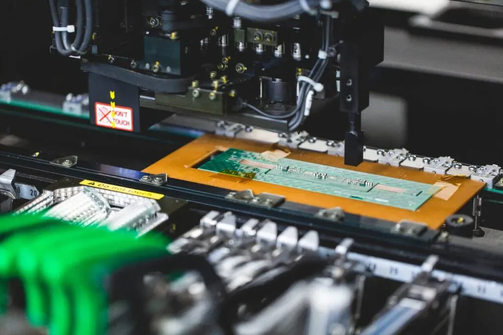
What Is the SMT Assembly Process and Why It Matters for Mobile Phones
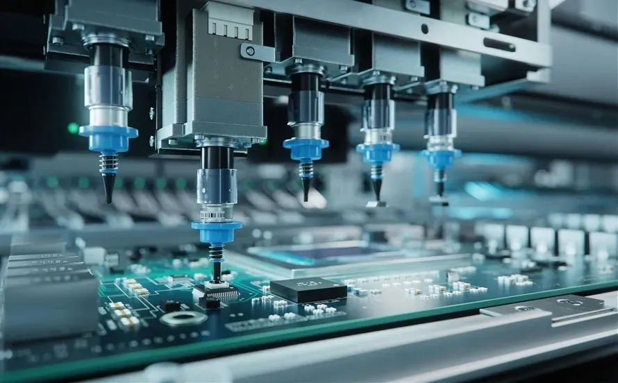
Surface Mount Technology, or SMT assembly process, involves printing solder paste on pads, placing components, and reflowing to bond them. Unlike through-hole methods, SMT allows components on both PCB sides, critical for slim mobile phone designs. This process supports fine-pitch parts like 0201 resistors and BGAs, fitting billions of transistors into smartphone processors. Reliability hinges on each step, as defects amplify in field use under vibration and heat cycles. For electric engineers, mastering SMT reduces rework costs and meets tight delivery schedules. Wave soldering complements SMT for selective through-hole parts, though SMT reflow handles most mobile PCB needs.
Solder Paste Application: Foundation of Reliable Joints
Solder paste application begins with stencil printing, where a metal stencil aligns over the PCB to deposit paste via squeegee pressure. Paste composition, typically 85 to 90 percent metal powder in flux, must match alloy like SAC305 for lead-free compliance. Uniform thickness, around 100 to 150 microns, prevents bridging or insufficient joints during reflow soldering PCB. Engineers inspect paste volume using SPI systems to catch variations early. Cleanliness of stencils and boards prevents contamination, which could cause voids. Proper viscosity control ensures release from stencil apertures without smearing.
Stencil design incorporates trapezoidal apertures for better paste release on fine-pitch pads. Registration accuracy below 25 microns aligns paste with pads, vital for component placement accuracy later. Overprinting risks shorts, while underprinting leads to open joints post-reflow. Humidity control in the print area stabilizes paste rheology. Troubleshooting paste slumping involves adjusting squeegee speed and pressure. These steps set the stage for flawless SMT assembly process execution.
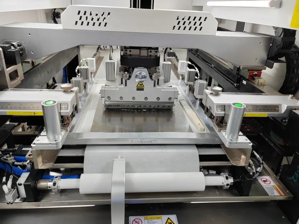
Achieving Component Placement Accuracy in SMT
Component placement accuracy defines SMT success, targeting plus or minus 50 microns for most mobile phone parts. High-speed pick-and-place machines use vision systems to correct offsets from fiducials on the PCB. Fine-pitch QFNs and BGAs demand sub-30 micron precision to avoid shifted joints in reflow soldering PCB. Feeders supply taped components, with nozzle changes for varied sizes from 01005 to large shields. Engineers calibrate machines daily to counter thermal expansion mismatches between feeders and boards. Placement speed balances with accuracy, often exceeding 100,000 chips per hour in volume runs.
Post-placement AOI verifies positions before reflow, flagging misplacements or polarity errors. Multi-head turrets optimize throughput for mixed assemblies. Vibrations from transport can shift parts, so gentle handling prevails. For BGAs, underfill preparation follows placement if needed for enhanced reliability. Accuracy logs guide process tweaks, correlating with yield data. This precision ensures joints withstand drop tests and thermal cycling in phones.
Reflow Soldering PCB: Thermal Profile Mastery
Reflow soldering PCB heats the assembly in a conveyor oven to liquefy solder paste, forming intermetallic bonds. The profile follows J-STD-020 standards, with preheat ramping 1 to 3 degrees C per second to 150 degrees C. Soak at 150 to 180 degrees C activates flux and equalizes temperatures across the board. Peak reflow hits 235 to 260 degrees C for 40 to 90 seconds above liquidus, melting SAC alloys without damaging components. Cooling solidifies joints, ideally 2 to 4 degrees C per second to minimize thermal shock. Engineers profile ovens with thermocouples on test boards to validate uniformity.
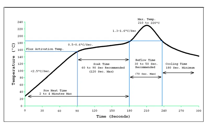
Nitrogen atmospheres reduce oxidation, improving wetting on fine pitches. Profile deviations cause tombstoning, where components lift due to uneven heating. IPC-A-610 criteria inspect post-reflow joints for fillet shape and voiding. Convection ovens dominate for precise control over IR types. Time above liquidus (TAL) metrics track solder flow completeness. Mastering these ensures void-free joints under mobile phone operating stresses.
Wave Soldering: When and How It Fits Mobile PCB Assembly
Wave soldering suits through-hole components, flooding pins with molten solder via a pumped wave. In mobile phones, it handles connectors or large electrolytics post-SMT reflow, using selective pallets to protect surface mounts. Flux spray pre-cleans pins, with preheat stabilizing boards at 100 to 130 degrees C. Dwell time over the wave, 3 to 5 seconds, forms fillets per IPC-A-610. Nitrogen shrouds minimize dross and bridging. Engineers prefer it for mixed-technology boards where full SMT proves costly.
Turbo pallets shield SMT areas, aligning precisely with board edges. Solder pot temperatures hover at 250 to 260 degrees C for eutectic or lead-free alloys. Post-wave cleaning removes flux residues to prevent corrosion. Compared to reflow soldering PCB, wave excels in volume for TH parts but risks shadowing on dense boards. Drag soldering variants aid fine-pitch headers. Integration with SMT demands sequence planning to avoid reflow rework on wave joints.
Best Practices for Mobile Phone PCB Assembly
Align processes to IPC-J-STD-001 requirements for soldered assemblies, ensuring workmanship consistency. Maintain ESD controls throughout, grounding operators and ionizers neutralizing charges on components. Bake hygroscopic parts per J-STD-020 to below 0.1 percent moisture before reflow soldering PCB. Solder paste storage at 5 to 10 degrees C with 24-hour warm-up prevents brittleness. Daily first-article inspections catch stencil wear or feeder jams early. Yield tracking via SPC identifies drifts in component placement accuracy.
Cleanroom class 1000 environments curb particle contamination during solder paste application. Reflow profiling every shift validates thermal stability. AOI and AXI integrate for 100 percent inspection on critical nets. Rework stations with hot air tools fix isolated defects without broad heating. Documentation of process parameters aids audits and scaling. These practices boost first-pass yields above 98 percent in production.
Troubleshooting Common SMT Assembly Issues
Tombstoning arises from rapid preheat ramps vaporizing flux unevenly, lifting chip ends; extend soak time to equalize. Solder beading from excessive paste volume demands stencil thickness audits. Bridging on QFPs traces to paste smearing, resolved by finer apertures or snap-off distances. Head-in-pillow defects, where BGA balls fail to merge with paste, stem from profile mismatches; align peak temperatures precisely. Voids over 25 percent area per IPC-A-610 trigger profile or paste adjustments. Component shift post-placement signals feeder vibrations; secure tape paths and verify vacuum levels.
Warpage exceeding 0.75 percent I/100mm hampers reflow, measured via shadow moire per IPC-TM-650. Insufficient wetting from oxidized pads requires flux potency checks. Post-reflow cracking links to cooling rates; gradual profiles prevent brittle intermetallics. Cross-section analysis confirms root causes. Iterative DOE refines parameters. Proactive SPC prevents escalations.
Conclusion
The SMT assembly process, anchored by precise solder paste application and reflow soldering PCB, drives mobile phone PCB reliability. Component placement accuracy and thermal profiling per standards like J-STD-020 ensure robust joints under real-world stresses. Wave soldering supplements for hybrid boards, demanding careful integration. Best practices and troubleshooting minimize defects, aligning with IPC guidelines. Engineers applying these insights achieve higher yields and durable products. Continuous process verification sustains quality in evolving mobile designs.
FAQs
Q1: What factors most affect component placement accuracy in the SMT assembly process?
A1: Component placement accuracy depends on machine vision calibration, fiducial registration, and feeder stability. Vibrations or thermal drifts shift offsets, while nozzle vacuum issues drop parts. Engineers verify with AOI post-placement, targeting under 50 microns for mobile fine-pitch. Process controls like daily offsets and speed throttling maintain precision in high-volume runs.
Q2: How does the reflow soldering PCB profile influence joint quality?
A2: Reflow soldering PCB profiles control preheat, soak, peak, and cool phases per J-STD-020 to avoid defects like voids or tombstoning. Insufficient TAL causes incomplete melting, while excessive peaks damage components. Nitrogen use enhances wetting. Profiling with board-mounted thermocouples ensures uniformity across dense mobile PCBs.
Q3: Why is solder paste application critical before reflow soldering PCB?
A3: Solder paste application via stencil sets paste volume and alignment for reliable joints in SMT assembly process. Variations lead to bridging or opens post-reflow. SPI verifies deposit height and area. Proper rheology prevents slumping, ensuring fine-pitch accuracy for mobile components.
Q4: When should wave soldering be used alongside SMT in mobile phone PCBs?
A4: Wave soldering applies to through-hole parts like connectors after SMT reflow, using pallets to shield surface mounts. It excels for high-pin-count TH but risks flux residues. Preheat and dwell optimize fillets per IPC-A-610. Selective use maintains hybrid assembly efficiency.
References
IPC-A-610H — Acceptability of Electronic Assemblies. IPC, 2019
J-STD-020E — Moisture/Reflow Sensitivity Classification for Nonhermetic Surface Mount Devices. JEDEC, 2014
IPC-J-STD-001H — Requirements for Soldered Electrical and Electronic Assemblies. IPC, 2018