Introduction
CEM-1 PCBs represent a cost-effective choice for single-layer applications in consumer electronics and simple control circuits. Engineers designing with this material must prioritize trace width and spacing to ensure reliable current handling, voltage isolation, and signal integrity. Proper optimization prevents overheating, short circuits, and performance degradation in compact layouts. This article explores CEM-1 design guidelines, including principles for PCB trace spacing for CEM-1 and single-layer PCB current capacity. By mastering these elements, electric engineers can achieve robust designs compliant with industry standards. Focus on PCB impedance matching further enhances functionality for moderate-frequency signals.
Understanding CEM-1 and Its Design Challenges
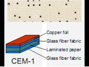
CEM-1 consists of a paper-based core reinforced with woven glass and epoxy on the surfaces, distinguishing it from higher-performance laminates. This composition yields a dielectric constant around 4.2 to 5.0 at 1 MHz, suitable for low-frequency operations but limiting high-speed applications. Single-layer construction amplifies the importance of trace width and spacing, as there are no inner layers for additional routing or shielding. Engineers encounter challenges like lower thermal conductivity compared to glass-epoxy alternatives, affecting heat dissipation from traces. Adhering to CEM-1 design guidelines ensures mechanical stability and electrical performance under operating conditions. Visual representation aids comprehension of material layers.
Trace width directly influences resistance and current capacity, while spacing governs dielectric breakdown risks. In single-layer CEM-1 boards, traces occupy the primary copper layer, making efficient use of space critical. Poor spacing can lead to crosstalk or arcing, especially in humid environments where CEM-1's hygroscopic nature plays a role. Current capacity calculations account for copper thickness, typically 1 oz/ft2, and allowable temperature rise. These factors demand precise engineering to balance density and reliability.
Technical Principles of Trace Width in CEM-1 PCBs
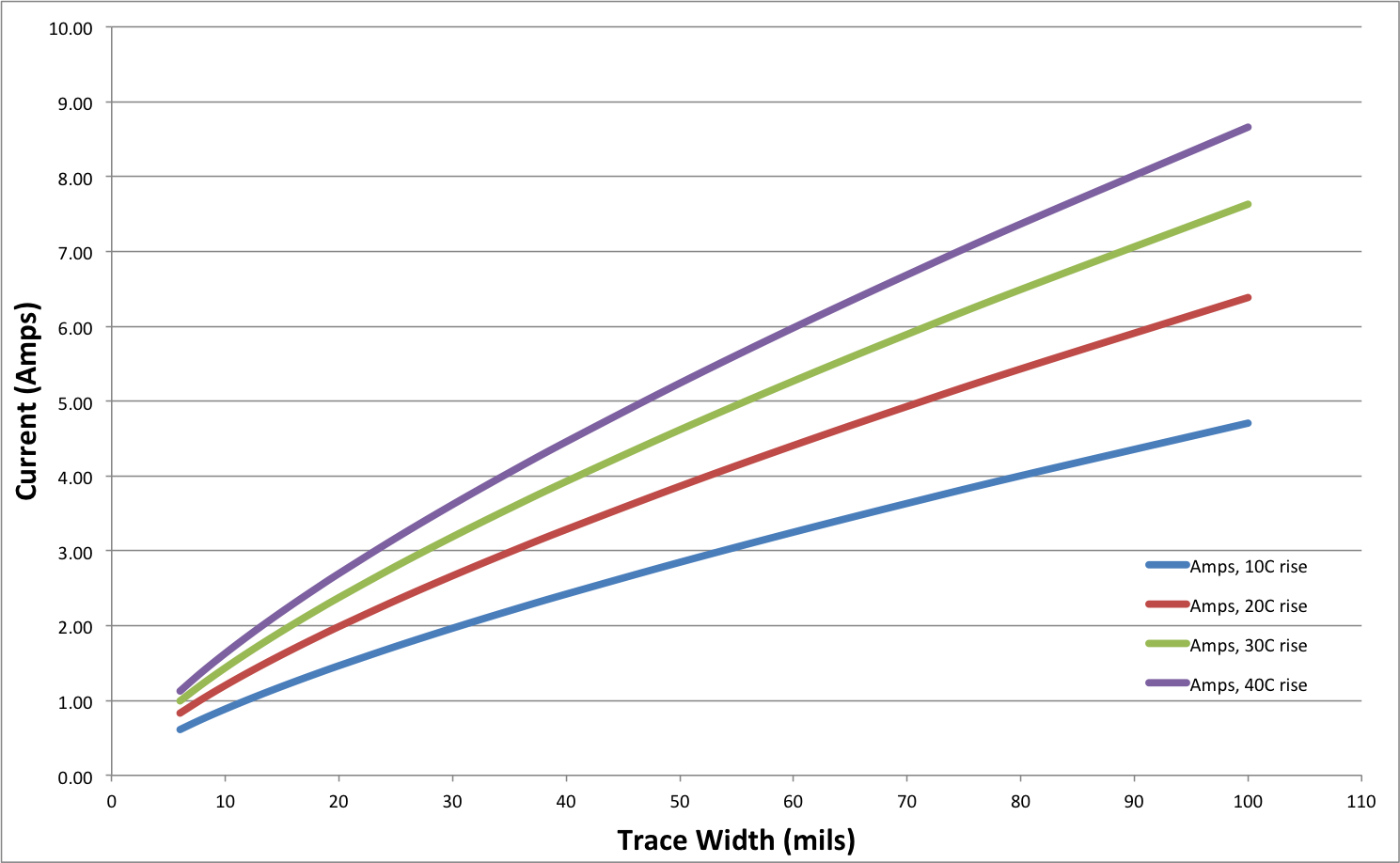
Trace width determination in CEM-1 PCBs relies on current-carrying capacity, governed by thermal management principles. Wider traces reduce resistance and heat generation via lower current density, crucial for single-layer PCB current capacity. IPC-2221 provides generic guidelines for calculating external trace widths based on operating current, ambient temperature, and maximum rise. The standard emphasizes cross-sectional area, where width multiplies by copper thickness to handle power without excessive heating. For CEM-1, the substrate's moderate thermal properties necessitate conservative margins to avoid board-level hotspots.
Engineers use CEM-1 PCB trace width calculators derived from these standards to input parameters like current and temperature rise for instant results. These tools apply empirical formulas correlating area to current, ensuring traces dissipate heat effectively into the air and board. Single-layer designs treat all traces as external, simplifying but heightening sensitivity to airflow and component proximity. Variations in copper plating uniformity further underscore the need for validated calculations. By integrating these principles, designs maintain integrity across production batches.
PCB Trace Spacing for CEM-1: Voltage and Isolation Essentials
Spacing between traces in CEM-1 PCBs prevents electrical breakdown, following clearance and creepage rules scaled to voltage levels. IPC-2221 outlines minimum distances for external conductors, factoring in pollution degree and coating presence. For low-voltage applications common in CEM-1 boards, spacing exceeds trace width to minimize field concentration and partial discharge risks. The material's dielectric strength supports moderate voltages, but spacing must account for manufacturing tolerances like etching undercuts.
In humid conditions, CEM-1 absorbs moisture, potentially reducing insulation resistance and demanding increased spacing. Creepage paths along surfaces require longer distances than air clearances, especially near edges or solder masks. Engineers calculate these using standard tables, adjusting for altitude and contamination levels. Proper spacing also aids inspectability during quality control. This structured approach aligns with CEM-1 design guidelines for long-term reliability.
Single-Layer PCB Current Capacity Considerations
Single-layer CEM-1 PCBs carry current primarily through surface traces, where capacity depends on width, thickness, and environmental factors. Heat primarily convects to ambient air, with limited substrate conduction due to CEM-1's properties. Standards like IPC-2221 recommend derating for multilayer absence, prioritizing wider traces for power paths. Temperature rise directly impacts component longevity, necessitating simulations or calculators for validation. Engineers balance capacity with board size, often segmenting high-current lines.
Plating thickness variations during fabrication influence resistance, so designs incorporate safety factors. For power distribution, multiple parallel traces enhance capacity without excessive width. Monitoring junction temperatures near traces prevents failures. These practices optimize single-layer PCB current capacity effectively.
PCB Impedance Matching in CEM-1 Designs
Impedance matching in CEM-1 PCBs ensures signal integrity for digital or RF interfaces on single layers. Microstrip configuration dominates, where trace width, substrate height, and dielectric constant dictate characteristic impedance. CEM-1's Er around 4.5 requires wider traces for 50-ohm lines compared to lower-Er materials. Calculators input stack-up details to compute widths, maintaining return loss below thresholds.
Fabrication tolerances affect impedance variation, so CEM-1 design guidelines suggest controlled copper weights and etching. Solder mask layers slightly alter effective Er, demanding post-layout verification. For mixed-signal boards, spacing isolates controlled-impedance traces from power lines. This precision elevates performance in cost-sensitive applications.
Practical Best Practices for CEM-1 Trace Optimization
Start with CEM-1 PCB trace width calculators to establish baselines for all nets, inputting realistic currents and 10-20°C rises. Assign wider widths to power traces, tapering signal lines for density. Maintain spacing at least equal to width, increasing for higher voltages per IPC-2221. Route high-current paths away from heat-sensitive components, leveraging board edges for cooling.
Incorporate annular rings adequately around pads to avoid trace narrowing. Validate designs with DRC rules mirroring standards. Prototype testing measures actual resistance and temperature. Iterative refinement ensures manufacturability. These steps form core CEM-1 design guidelines.
- Minimum Trace Width — Based on current and IPC-2221
- Minimum Spacing — Voltage-dependent clearance
- Copper Thickness — 1 oz/ft2 standard
- Impedance Target — Calculate for microstrip
Troubleshooting Common Issues
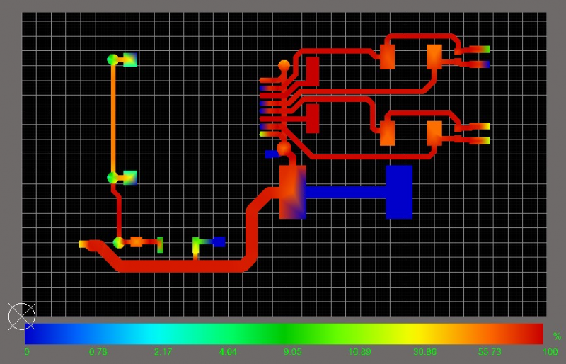
Overheating often signals inadequate trace width; infrared imaging reveals hotspots during load tests. Arcing from tight spacing appears as carbon tracks post-failure. Impedance mismatches cause ringing, verifiable via TDR. Moisture ingress exacerbates CEM-1 issues, prompting conformal coatings. Systematic checks per standards resolve these.
Conclusion
Mastering trace width and spacing optimizes CEM-1 PCB designs for reliability and efficiency. Key principles from IPC-2221 guide current capacity, isolation, and impedance control. Practical calculators and best practices enable electric engineers to navigate single-layer constraints. Implementing these CEM-1 design guidelines yields cost-effective, high-performance boards. Prioritize validation to meet application demands consistently.
FAQs
Q1: What is a CEM-1 PCB trace width calculator and how does it work?
A1: A CEM-1 PCB trace width calculator uses IPC-2221 formulas to determine minimum widths based on current, copper thickness, and temperature rise. Engineers input parameters for single-layer external traces, receiving optimized dimensions to prevent overheating. This tool accounts for CEM-1's thermal limits, ensuring reliable power handling in low-cost designs. It streamlines adherence to CEM-1 design guidelines.
Q2: How do you calculate single-layer PCB current capacity for CEM-1?
A2: Single-layer PCB current capacity follows IPC-2221 charts for external traces, factoring width, thickness, and allowable Delta-T. Wider traces increase cross-section, dissipating heat via convection. For CEM-1, conservative ratings suit its substrate properties. Use calculators for precise values, verifying with thermal analysis.
Q3: What are key PCB trace spacing for CEM-1 rules?
A3: PCB trace spacing for CEM-1 follows IPC-2221 clearance tables, scaled to voltage and pollution degree. Minimum distances prevent breakdown, exceeding trace widths typically. Adjust for creepage in humid setups. These rules support safe operation in single-layer boards.
Q4: How does PCB impedance matching apply to CEM-1 designs?
A4: PCB impedance matching in CEM-1 uses microstrip equations with Er ≈ 4.5, calculating trace widths for targets like 50 ohms. Tools adjust for height and mask effects. Proper matching minimizes reflections in signal paths, vital for moderate speeds.
References
IPC-2221B — Generic Standard on Printed Board Design. IPC, 2003
IPC-6012E — Qualification and Performance Specification for Rigid Printed Boards. IPC, 2015
IPC-A-600K — Acceptability of Printed Boards. IPC, 2020