What Role Does Prepreg Play in High-Speed PCB Design?
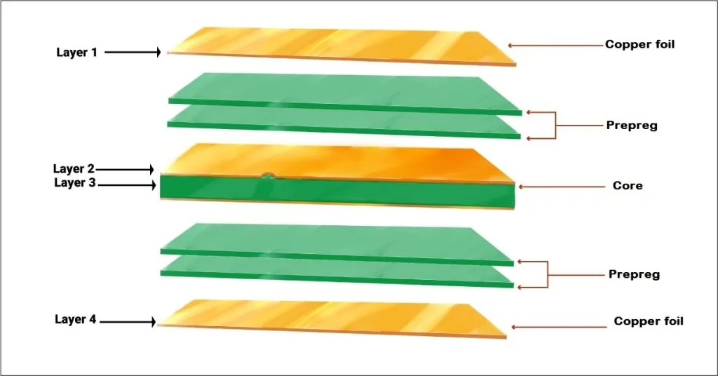
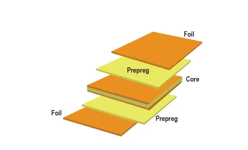
Prepreg, short for "pre-impregnated material," is a vital component in the construction of multilayer printed circuit boards. It consists of a fiberglass weave saturated with a resin and then partially cured. Its primary functions are to serve as an electrical insulator between conductive layers and to act as a bonding agent that holds the PCB stack-up together during the lamination process.
In high-speed applications, where electrical signals travel at incredibly fast rates, the properties of prepreg become critically important. It directly influences the dielectric constant (Dk) and loss tangent (Df) of the board, which are key parameters affecting how signals propagate, how quickly they travel, and how much energy they lose.
Impact on Signal Integrity
For circuits operating at frequencies exceeding 1 GHz, even minor inconsistencies in prepreg characteristics can lead to significant signal degradation. Issues like signal distortion, unwanted crosstalk between traces, or impedance mismatches can severely compromise performance. Selecting appropriate prepreg materials and thicknesses is thus essential to preserve signal integrity, ensuring data remains clear and reliable in demanding high-speed environments.
What Factors Influence Prepreg Thickness in High-Speed PCBs?
Deciding on the correct prepreg thickness for high-speed PCBs involves balancing various electrical performance requirements with mechanical stability and manufacturing practicalities. It’s a nuanced decision where several key aspects must be carefully weighed.
Managing Impedance and Dielectric Spacing
Maintaining controlled impedance is paramount in high-speed designs to prevent signal reflections that can corrupt data. The thickness of the prepreg layer directly dictates the characteristic impedance of signal traces. For example, a thinner dielectric layer generally results in lower impedance for a given trace width, while a thicker layer increases it. Common impedance targets for high-speed protocols like USB 3.0 or PCIe are 50 ohms for single traces and 100 ohms for differential pairs. Achieving these values requires precise calculation of prepreg thickness, often using specialized software that considers the material’s dielectric constant, which typically ranges from 3.5 to 4.5 for standard FR-4.
Signal Propagation Speed and Timing
The thickness of the prepreg also has a direct bearing on signal propagation delay, which is the time a signal takes to travel along a trace. Thicker prepreg layers increase the distance between signal planes and their corresponding ground references. This elongated path through the dielectric material can slightly slow down signal transmission. In timing-sensitive applications such as DDR4 memory or 5G communication, where signals can reach 10 GHz or higher, even a fractional difference in prepreg thickness (e.g., 0.025 mm) can impact critical timing margins. Consequently, thinner prepreg layers (e.g., 0.05 mm to 0.075 mm) are often favored to minimize delay.
Mitigating Signal Loss and Dielectric Properties
Signal loss is a significant concern in high-speed PCB design, and the material properties of the prepreg are a major contributor. The loss tangent (Df) of the prepreg indicates how much signal energy is converted into heat. Standard FR-4 prepreg has a Df of approximately 0.02, which can lead to noticeable signal attenuation at frequencies above 5 GHz. For applications demanding higher performance, low-loss prepreg materials with a Df of 0.005 or even lower are frequently recommended. Additionally, using thinner prepreg layers can lessen signal loss by reducing the volume of dielectric material the signal must traverse, although extremely thin layers (below 0.05 mm) can introduce manufacturing complexities and higher costs.
Ensuring Mechanical Strength and Board Structure
While thinner prepreg layers often benefit electrical performance, they can sometimes compromise the mechanical robustness of the PCB. Thicker prepreg layers, such as those ranging from 0.125 mm to 0.2 mm, provide enhanced structural integrity, particularly for boards with numerous layers or those exposed to physical stress. Designers must carefully balance electrical requirements with the need for mechanical reliability. In a typical 8 layer PCB , a combination of prepreg thicknesses might be employed: thinner layers near critical signal paths for impedance control, and thicker layers around power and ground planes for improved stability.
Manufacturing Feasibility and Cost Implications
The availability and cost-effectiveness of various prepreg thicknesses also play a role in selection. Commonly available thicknesses, such as 0.1 mm or 0.15 mm, are generally easier and more economical to process. Custom or unusually thin prepreg layers, however, can lead to longer lead times and increased manufacturing costs. Very thin prepregs (below 0.05 mm) can also be challenging to handle during the lamination process, potentially increasing the risk of manufacturing defects like voids or delamination. Engaging with your online pcb manufacturer early in the design phase can help identify practical prepreg options that align with both performance targets and budgetary constraints.
How Prepreg Material Properties Influence High-Speed Signals
Beyond its physical thickness, the inherent material characteristics of prepreg are equally critical for preserving signal integrity in high-speed designs. A deeper understanding of these properties is key to making informed material choices.
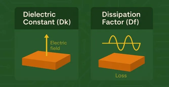
Dielectric Constant (Dk)
The dielectric constant (Dk) quantifies a material's ability to store electrical energy and how much it slows down an electric field compared to a vacuum. In high-speed PCBs, a lower Dk value (e.g., 3.0–3.5) is generally preferred because it enables signals to propagate faster, thereby reducing propagation delay. Standard FR-4 prepreg typically has a Dk in the range of 4.2–4.5, which may prove too high for applications exceeding 10 GHz. For ultra-high-speed designs, advanced prepreg materials with a Dk of 3.0 or less can significantly boost performance, though this often comes with a higher material cost.
Loss Tangent (Df)
As previously noted, the loss tangent (Df) indicates the rate at which signal energy is dissipated as heat within the dielectric material. A lower Df value is essential for minimizing signal loss, especially in high-frequency designs. For instance, at 10 GHz, using a prepreg with a Df of 0.003 can reduce signal attenuation by as much as 50% compared to standard FR-4, which typically has a Df of 0.02. Low-loss prepreg materials are indispensable for applications like radar systems or high-speed networking, where maintaining signal strength over extended trace lengths is a priority.
Thermal and Mechanical Durability
High-speed PCBs frequently operate in demanding environments, requiring prepreg materials that can withstand considerable thermal and mechanical stresses. A prepreg with a high glass transition temperature (Tg), typically 170°C or higher, helps ensure structural stability during the soldering process and throughout the board’s operational lifespan. Furthermore, it is important that the coefficient of thermal expansion (CTE) of the prepreg closely matches that of the copper and core layers to prevent issues such as warping or delamination of the PCB.
Suggested Reading: PCB Prepreg Thickness: A Designer's Guide to Stackup, Materials, and Performance
How Prepreg Thickness and Material Contribute to Signal Loss
Signal loss in high-speed PCBs originates from two main factors: conductor loss, due to the inherent resistance in copper traces, and dielectric loss, caused by energy dissipation within the prepreg material. While conductor loss can be mitigated through design choices such as using wider traces or smoother copper finishes, dielectric loss is profoundly influenced by both the thickness and material properties of the prepreg.
Thicker prepreg layers generally lead to increased dielectric loss because signals must traverse a greater volume of the dielectric material, resulting in more energy dissipation. For example, at 5 GHz, a 0.15 mm thick prepreg layer might incur 0.5 dB more loss per inch compared to a 0.075 mm layer of the same material. Opting for a thinner layer or a low-loss prepreg can significantly reduce this effect. Additionally, the inherent weave pattern of the fiberglass in standard prepreg can contribute to signal loss and timing skew in differential pairs. The uneven distribution of glass fibers can create localized variations in the dielectric constant along a trace, leading to timing mismatches between the differential signals. Advanced prepreg materials often address this by employing more uniform weaves or non-woven glass structures to mitigate these issues.


