Introduction
In modern electronics, multilayer printed circuit boards handle increasing power densities from components like processors and power converters. Effective heat spreading prevents hotspots that degrade performance and reliability. PCB layer stackup thermal design plays a central role by arranging copper planes and signal layers to distribute heat evenly. Poor stackup choices lead to thermal gradients, causing warpage or component failure. Optimizing layer arrangement enhances conduction through high-thermal-conductivity copper layers. This article explores principles and best practices for heat spreading in multilayer PCBs.
Understanding PCB Stackups and Their Role in Thermal Management
A PCB stackup defines the sequence of copper layers, dielectrics, and cores that form the board structure. In multilayer designs, inner layers often serve as power and ground planes, which excel at in-plane heat spreading due to copper's high thermal conductivity. Heat spreading in multilayer PCBs relies on these planes to conduct thermal energy laterally across the board, reducing peak temperatures at sources. Signal layers contribute less but require careful placement to avoid impeding heat paths. Industry standards like IPC-2221 outline guidelines for thermal management, emphasizing symmetrical arrangements to balance mechanical and thermal performance. Why it matters: suboptimal stackups increase junction temperatures, shortening component life and violating reliability specs.
Thermal vias bridge components to inner planes, enabling vertical heat transfer. Without optimized stackups, vias alone cannot compensate for poor layer sequencing. Engineers must consider dielectric thickness, as thinner cores between planes improve conduction while maintaining electrical isolation. Ground planes act as distributed heat sinks, coupling closely with power planes for efficient dissipation. Copper pour thermal performance improves with continuous, unsegmented areas that minimize resistance to heat flow.
Fundamental Principles of Heat Transfer in PCB Stackups
Heat transfer in PCBs follows conduction, primarily through Fourier's law, where flux depends on material conductivity, area, and temperature gradient. Copper planes dominate due to conductivity around 400 W/m·K, far exceeding dielectrics at 0.2-0.5 W/m·K. In stackups, heat from surface-mount devices spreads radially in planes before transferring to ambient via convection or external sinks. IPC-2221 details cooling mechanisms, including conduction paths optimized by adjacent power and ground layers. Radiation and convection play secondary roles, enhanced by surface copper pours.
Layer asymmetry causes warpage from CTE mismatches during reflow or operation. Symmetrical stackups, with mirror-image layers around the neutral axis, maintain flatness under thermal stress. Power plane design for thermal management positions high-current planes centrally to maximize spreading area. Ground planes as heat sinks leverage full-layer pours connected via stitching vias. Copper pour thermal performance scales with thickness; heavier copper (e.g., 2 oz/ft2) adds thermal mass and lowers resistance.
Vertical heat paths via thermal vias arrays connect hotspots to multiple planes, but stackup dictates overall efficacy. Dielectric materials with higher glass transition temperatures support elevated operating conditions. Conductor sizing per IPC-2152 ensures current-carrying capacity without excessive self-heating, integrating thermal derating factors.
Key Factors Influencing Heat Spreading Efficiency
Copper thickness and fill factor determine plane effectiveness. Full pours outperform partial ones by providing uniform spreading paths. In multilayer PCBs, interleaving signal layers with planes balances EMI control and thermal paths. Adjacent power-ground pairs form natural capacitors while aiding heat transfer through thin dielectrics. Voids or splits in planes create barriers, concentrating heat and risking delamination.
Thermal vias require plating for conductivity, often grouped in 0.5-1 mm pitch arrays under packages. Filled vias enhance performance but add cost. Ground plane as heat sink benefits from perimeter stitching to chassis grounds. PCB layer stackup thermal design simulations predict gradients, guiding iterations. Material selection influences via reliability under cycling.
Prepreg and core CTE alignment prevents microcracks. Thicker boards offer more planes but longer vertical paths, trading off efficiency.
Best Practices for Layer Arrangement in Multilayer Stackups
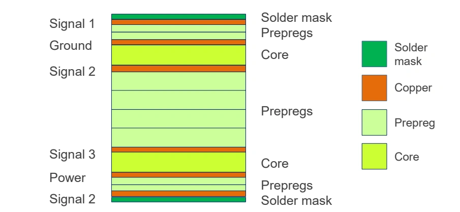
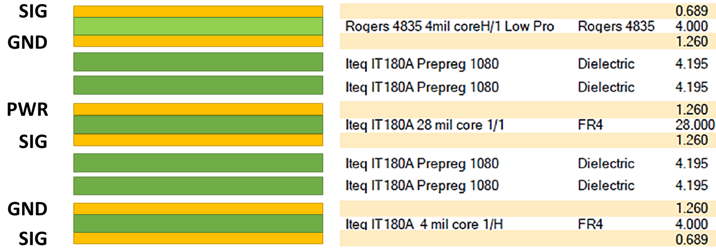
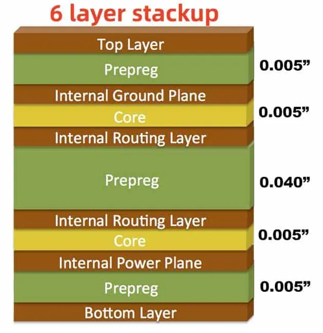
Start with even-layer counts for symmetry: 4-layer (signal-ground-power-signal), 6-layer (signal-ground-signal-power-signal-ground). Position power planes near heat sources, flanked by ground for coupling. Dedicate inner layers 2-3 for planes in 8+ counts to isolate signals outward. Maintain dielectric spacing under 0.2 mm between planes for low impedance and good conduction.
Use heavy copper (1-3 oz) on thermal planes; IPC-2221 recommends evaluating for heatsinking. Stitch planes with vias at 10-20 mm grid for equipotential and heat uniformity. Avoid routing signals over plane splits to prevent EMI and thermal bottlenecks. Copper pours on outer layers boost surface convection.
Related Reading: Mastering 12-Layer PCB Stackups for High-Performance High-Speed Designs
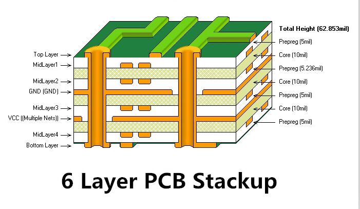
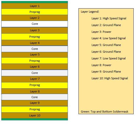
For high-power, embed planes symmetrically: top signal, ground, power, core, power, ground, signal. Thermal relief pads on vias prevent soldering shorts while allowing flow. Simulate stackups to verify <20°C rise targets.
Power Plane Design for Thermal Management
Power planes distribute current and spread heat from ICs and regulators. Full-sheet designs minimize voltage drop and hotspots. Pair with adjacent ground planes for field containment and conduction paths. Segmentation only where voltage domains require, bridged by capacitors.
Thicker copper reduces I2R losses, converting less to heat. Vias from components fan out to planes, maximizing contact. In stackups, central power layers access larger areas for spreading.
Related Reading: Impedance Control with Power Plane, design
Leveraging Ground Planes as Heat Sinks
Ground planes offer low-impedance returns and vast spreading surfaces. Connect all grounds to a single net, avoiding splits. Stitch edges to chassis for external sinking. In heat spreading in multilayer PCBs, grounds absorb flux from multiple sources, averaging temperatures.
Position grounds outermost or adjacent to signals for reference integrity. Copper pour thermal performance peaks in continuous grounds, outperforming traces by orders in conductivity.
Enhancing Copper Pour Thermal Performance
Copper pours fill unused areas, aiding local spreading. Maximize coverage, connecting to planes via vias. Heavier pours add mass, slowing transients. Avoid islands; merge into main nets.
On signal layers, pours act as shields while contributing modestly to thermal paths. Test configurations per JEDEC thermal boards for validation.
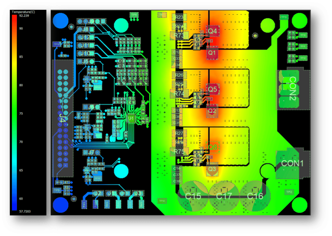
Case Study: Comparing 4-Layer vs. 8-Layer Stackups
Consider a power supply board with 50W dissipation. A 4-layer stackup (sig-gnd-pwr-sig) shows 15°C higher peaks than 8-layer (sig-gnd-sig-pwr-core-pwr-sig-gnd). The extra planes double spreading capacity, lowering gradients by 30%. Thermal vias to inner pairs prove decisive. Simulations confirm adherence to limits.
Symmetric 8-layer reduces warpage by half post-reflow. Ground plane as heat sink dominates dissipation.
Conclusion
Optimizing PCB layer stackup thermal design demands symmetrical arrangements, strategic plane placement, and vias. Power plane design for thermal management, ground plane as heat sink, and copper pour thermal performance integrate for robust spreading. Follow IPC guidelines for reliability. Engineers achieve cooler boards, extending life in demanding applications. Prioritize simulations and symmetry for success.
FAQs
Q1: What is the ideal layer arrangement for heat spreading in multilayer PCBs?
A1: Position power and ground planes adjacently and centrally in the stackup, with signal layers outward for symmetry. This setup maximizes in-plane conduction per IPC-2221 principles. Use thermal vias to link components. Symmetric designs prevent warpage. Aim for thin dielectrics between planes.
Q2: How does a ground plane function as a heat sink in PCB layer stackup thermal design?
A2: Ground planes spread heat laterally due to large copper area and low resistance. Stitch vias ensure uniform potential and flow to edges. Adjacent to power planes, they enhance coupling. Continuous pours outperform segmented ones. This reduces hotspots effectively in high-power boards.
Q3: Why is copper pour thermal performance critical in power plane design for thermal management?
A3: Copper pours provide low-resistance paths for radial spreading, lowering peak temperatures. Heavier fills add mass for stability. Connect to inner planes via vias. Avoid splits to maintain efficacy. Simulations verify gains in multilayer setups.
Q4: How do standards like IPC-2152 influence PCB stackup decisions for heat spreading?
A4: IPC-2152 guides conductor sizing to limit self-heating, informing plane thickness choices. It integrates with stackup for overall thermal budget. Derate for multilayer effects. Ensures current capacity without excessive rise. Complements JEDEC test methods.
References
IPC-2221B — Generic Standard on Printed Board Design. IPC, 2003
IPC-2152 — Standard for Determining Current Carrying Capacity in Printed Board Design. IPC, 2009
JEDEC JESD51-7 — High Effective Thermal Conductivity Test Board for Leaded Surface Mount Packages. JEDEC, 2004