What Are Prepreg and Dielectric Constant in PCB Manufacturing?
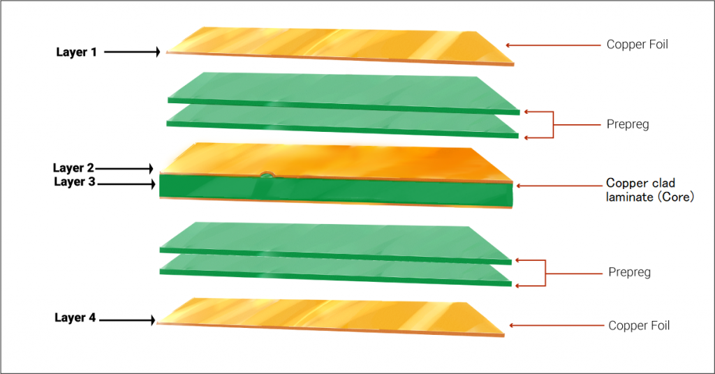
In the fabrication of printed circuit boards, "prepreg" refers to a fiberglass sheet that has been pre-impregnated with a resin system, partially cured to a B-stage. This material serves as an insulating layer between the copper traces of a multilayer PCB and acts as an adhesive, bonding layers together during the lamination process. Its characteristics fundamentally influence the board’s overall thickness and electrical behavior.
The dielectric constant (Dk), also known as relative permittivity, quantifies a material’s capacity to store electrical energy within an electric field. For prepreg, the Dk value directly affects how electrical signals propagate through the PCB. A lower Dk typically facilitates faster signal transmission, which is a critical attribute for circuits operating at high frequencies. Understanding and precisely controlling both the prepreg’s thickness and its Dk value are essential for achieving optimal PCB material properties and ensuring reliable electronic performance.
How Does Prepreg Thickness Influence PCB Design?
The physical thickness of the prepreg layer is a pivotal design parameter, directly dictating the spacing between conductive copper layers in a PCB stackup. This inter-layer distance significantly impacts various performance attributes, including impedance matching, signal integrity, and the board’s thermal management capabilities.
Critical Role in Impedance Control
In high-frequency pcb designs, maintaining consistent impedance across signal paths is non-negotiable for preserving signal integrity. Prepreg thickness is a direct determinant of the distance between a signal trace and its adjacent ground or power plane. Consequently, this spacing influences the characteristic impedance of the transmission line. For example, a thinner prepreg layer reduces the separation, leading to lower impedance, whereas a thicker layer increases it. Designers often specify particular impedance targets, such as 50 ohms for many radio frequency (RF) applications, and achieve this by meticulously selecting the appropriate prepreg thickness.
Impact on Signal Propagation and Thermal Stability
The thickness of the prepreg also affects signal propagation delays; a thicker layer means signals must traverse more dielectric material, potentially increasing delays. Conversely, while thinner prepreg reduces delays, it can exacerbate crosstalk if adjacent layers are brought too close. Achieving the right balance is crucial for high-frequency PCB performance. Beyond electrical characteristics, thicker prepreg layers can offer enhanced thermal dissipation and superior mechanical robustness, which are vital for boards subjected to elevated temperatures or significant physical stress. However, excessive thickness might result in a bulkier board, unsuitable for compact device requirements.
What Role Does Dielectric Constant (Dk) Play in Prepreg Materials?
The dielectric constant (Dk) of prepreg materials is a fundamental electrical property that profoundly impacts signal behavior, particularly in high-frequency applications. It quantifies a material's ability to concentrate electric flux, relative to a vacuum.
Affecting Signal Speed and Loss
A lower Dk value allows electrical signals to travel at a faster speed through the prepreg. This is because a reduced Dk diminishes the capacitance between signal traces, leading to less energy storage and quicker signal propagation. For high-frequency designs, materials with Dk values ranging from 2.2 to 3.0 are often favored over standard materials (Dk 4.4 to 4.8) to minimize signal delay. Furthermore, materials with lower Dk values typically exhibit a lower dissipation factor (Df), which translates to reduced signal loss due to energy absorption within the material—a critical factor for maintaining signal integrity over extended trace lengths.
Implications for Impedance Matching
The Dk value is also a key factor in determining the characteristic impedance of transmission lines within the PCB. Any significant mismatch in Dk between different dielectric materials within the board’s stackup can lead to signal reflections and degradation, compromising overall circuit performance. Therefore, precise control over the prepreg’s Dk is essential for effective impedance matching and reliable signal transmission.
How Prepreg Thickness and Dk Interact in High-Frequency PCB Design
For printed circuit boards operating at high frequencies, the interplay between prepreg thickness and its dielectric constant is especially significant. These two parameters collectively dictate how electrical signals behave as they traverse the board’s intricate pathways.
Joint Influence on Impedance and Signal Integrity
Both the physical thickness and the Dk value of the prepreg contribute to the characteristic impedance of a transmission line. For a given trace width, a thinner prepreg combined with a higher Dk tends to increase capacitance, thus lowering impedance. Conversely, a thicker prepreg with a lower Dk typically decreases capacitance, which results in higher impedance. Design engineers frequently employ sophisticated simulation tools to accurately model these complex interactions and select the optimal combination of parameters for their specific operating frequency range. At frequencies exceeding 1 GHz, even minor deviations in either prepreg thickness or Dk can lead to noticeable signal delays or losses.
Mitigating Crosstalk and Noise
The relationship between prepreg thickness and Dk also impacts signal isolation. Thinner prepreg layers coupled with high Dk values can intensify crosstalk between adjacent signal traces due to increased capacitive coupling. Conversely, while thicker layers with lower Dk values can effectively reduce crosstalk, they might not be suitable for compact designs where space is a premium. To optimize overall performance, designers must meticulously select materials and design the stackup to balance these factors, aligning with the specific operating frequency and application requirements.
Selecting Optimal Prepreg Materials for Your PCB Project
Choosing the right prepreg material for your PCB design involves a thorough evaluation of both its thickness and dielectric constant, tailored to your specific application needs. AIVON provides a comprehensive range of prepreg options and expert guidance to help designers make informed decisions.
Aligning Material Properties with Frequency Requirements
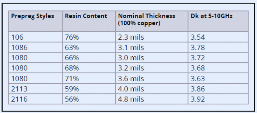
For lower-frequency applications (below 1 GHz), standard prepreg materials with Dk values around 4.4 and moderate thicknesses (e.g., 0.2-0.3 mm) are typically sufficient. However, for high-frequency designs (above 1 GHz), it becomes crucial to consider advanced materials featuring lower Dk values (ideally below 3.0) and thinner layers (e.g., 0.1-0.2 mm) to minimize signal loss and ensure high-speed performance.
Practical Tips for Material Selection
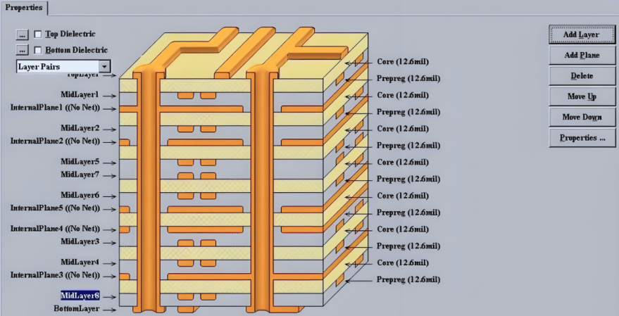
When designing multilayer boards, ensure consistency in prepreg thickness and Dk across all layers to prevent impedance mismatches that could degrade signal integrity. Utilizing simulation software to model various stackup configurations before manufacturing is a recommended best practice. While low-Dk materials and ultra-thin prepreg layers can significantly enhance performance, they often come with a higher PCB cost. It's important to weigh these performance gains against the added expense for your specific application. Always consult the manufacturer’s data sheets for detailed material properties, including Dk, dissipation factor, and available thicknesses, as these specifications are vital for predicting material behavior in your design.
Best Practices for High-Frequency PCB Design
Achieving optimal performance in high-frequency PCB designs extends beyond just selecting the right prepreg. Several additional best practices are essential to ensure signal integrity and overall reliability.
Addressing Signal Integrity Challenges
To minimize the fiber weave effect—where variations in the fiberglass weave of prepreg can cause signal skew in differential pairs—consider rotating trace routing or utilizing materials with more uniform weave patterns. Implement controlled impedance routing by designing traces with precise widths and spacing that account for prepreg thickness and Dk to match target impedance values. For instance, a 50-ohm trace in a 5 GHz application might require a specific width with a particular prepreg thickness and Dk.
Enhancing Grounding and Validation
Solid ground planes are crucial for reducing noise and providing clear return paths for signals. Ensure that the prepreg thickness between signal layers and ground planes is consistent to maintain uniform impedance across the board. Finally, utilize simulation tools to predict signal behavior before fabrication. Post-manufacturing, validate your designs through testing methods like time-domain reflectometry (TDR) to verify impedance characteristics and signal integrity, ensuring the board meets its performance specifications.
Overcoming Common Design Hurdles with Prepreg and Dk
Despite meticulous planning, designers frequently encounter specific challenges related to prepreg and dielectric properties. Addressing these issues proactively can prevent costly revisions and delays.
Mitigating Material Inconsistencies
One common challenge is the potential for inconsistent Dk values across different prepreg batches, which can disrupt impedance control. To counteract this, work with reputable suppliers, like AIVON, who ensure material consistency and specify strict tolerances for Dk in your design requirements. Another issue arises with ultra-thin prepreg layers, which can be difficult to handle during manufacturing and may increase the likelihood of defects. If such thin layers are essential for your design, close collaboration with your fabrication partner is key to ensuring process capability.
Addressing Signal Loss at Elevated Frequencies
If signal losses at high frequencies are greater than anticipated, consider transitioning to a prepreg material with a lower Dk and dissipation factor (Df). Even a modest reduction, such as moving from a Dk of 3.5 to 3.0, can yield a noticeable improvement at frequencies exceeding 5 GHz. Resolving these material-related challenges early in the design cycle is critical for optimizing production efficiency and achieving the desired performance outcomes.
Conclusion: Making Informed Choices for Superior PCB Performance
In the intricate realm of printed circuit board design, seemingly minor details like prepreg thickness and dielectric constant wield significant influence over overall performance, especially in high-frequency applications. A thorough understanding of how these factors interact—impacting signal integrity, impedance, and board reliability—empowers designers to make well-informed decisions that optimize their circuits. Whether the goal is to achieve minimal signal loss in advanced 5G communication systems or precise impedance control in sensitive RF circuits, the judicious selection of prepreg Dk value and thickness is a pivotal step.
AIVON is dedicated to supporting designers with premium-quality materials and expert consultation. By applying the insights discussed, you can elevate your high-frequency PCB design process and attain exceptional results. Always remember to balance performance demands with practical considerations such as cost and manufacturability, and rigorously validate your material choices through comprehensive simulation and testing. By adopting a strategic approach to PCB material properties, your designs can unlock their full potential, delivering the speed, dependability, and efficiency indispensable in today's sophisticated electronic devices.


