Introduction
Industrial automation controllers rely on printed circuit boards (PCBs) to manage complex operations in demanding environments. These PCBs integrate high-power processors, power management circuits, and sensors that generate significant heat during continuous operation. Effective thermal management ensures component longevity, prevents performance degradation, and maintains system reliability. Poor heat control can lead to hotspots, accelerated aging, and unexpected failures in automation systems. PCB thermal analysis plays a crucial role in identifying risks early in the design phase. By optimizing heat dissipation in PCBs, engineers can achieve higher uptime and compliance with operational demands.
Why Thermal Management Matters in Industrial Automation Controller PCBs
Industrial automation controllers operate in enclosures with limited airflow, amplifying thermal challenges. Heat buildup from power electronics and digital logic exceeds safe limits, causing electromigration, solder joint fatigue, and dielectric breakdown. Reliable thermal design directly impacts mean time between failures (MTBF), a key metric for automation uptime. Engineers must prioritize heat dissipation in PCBs to avoid derating components below their rated capacities. In high-density boards, thermal vias and strategic layouts become essential for uniform temperature distribution. Neglecting these aspects risks costly downtime in manufacturing lines or process control systems.
Fundamentals of Heat Generation and Transfer in PCBs
Heat in PCBs arises primarily from resistive losses in conductors, switching transients in semiconductors, and power dissipation in passives. Conduction dominates within the board, facilitated by copper traces, planes, and vias, while convection and radiation assist at surfaces. Thermal resistance, measured in degrees per watt, quantifies barriers to heat flow from junctions to ambient. Copper's high thermal conductivity spreads heat laterally, but thin layers limit effectiveness without enhancements. In multilayer stacks, inner planes act as heat spreaders, bridging hotspots to outer layers. Understanding these mechanisms guides PCB thermal analysis for predictive modeling.
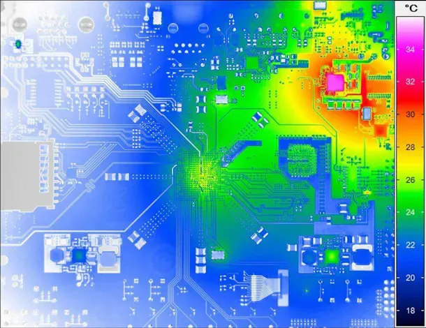
PCB Thermal Analysis Techniques
PCB thermal analysis employs finite element analysis (FEA) to simulate temperature profiles under load conditions. Engineers model material properties, boundary conditions, and power inputs to predict hotspots and gradients. Experimental validation uses infrared thermography for non-contact mapping or thermocouples for point measurements. These techniques reveal via effectiveness and plane contributions to overall dissipation. Adhering to guidelines in IPC-2221 ensures consistent design practices for thermal relief. Iterative analysis refines layouts before prototyping, minimizing revisions.
Implementing Thermal Vias for Enhanced Heat Dissipation
Thermal vias transfer heat vertically through the PCB stackup, connecting surface pads to inner copper planes. Arrays of 0.3 mm to 0.5 mm vias under heat-generating components maximize conductance without excessive board area. Filling vias with conductive epoxy reduces air gaps, improving reliability under thermal cycling. Placement near pinouts or thermal pads prevents localized overheating in controllers. IPC-2221 recommends via patterning to balance electrical and thermal functions. Proper tenting of soldermask preserves via integrity during assembly.
Heat dissipation in PCBs improves further with via stitching along high-current traces, distributing Joule heating. Engineers calculate via thermal resistance based on diameter, plating thickness, and count to meet design margins. In industrial applications, these features support sustained operation at elevated loads. Combining vias with cutouts enhances airflow paths. Validation through PCB thermal analysis confirms predicted performance.
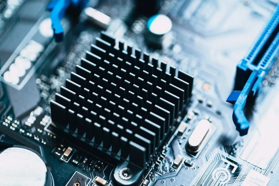
Heat Sink Design for PCBs in Demanding Environments
Heat sink design for PCBs involves selecting profiles that match board constraints and airflow availability. Pin-fin or plate-fin geometries increase surface area for convection, with base materials like aluminum offering good conductivity-to-weight ratios. Mechanical attachment via clips, screws, or adhesives ensures low interface resistance. Thermal interface materials fill gaps between component and sink, critical for flatness variations. Optimizing fin spacing balances airflow impedance and dissipation efficiency.
In industrial automation controllers, heat sinks interface directly with PCB-embedded heatsinks or chassis. Designers account for natural or forced convection in enclosures. PCB thermal analysis simulates sink contributions, guiding size and placement. Integration requires pad design for uniform contact pressure. Standards like IPC-2152 inform trace widths adjacent to sinks, preventing hotspots.
Selecting High-Temperature PCB Materials
High-temperature PCB materials withstand prolonged exposure without softening or delaminating. Standard FR-4 suits moderate environments, but controllers demand resins with elevated glass transition points for stability. Polyimide-based laminates offer superior performance in harsh thermal profiles, maintaining mechanical integrity. Ceramic-filled epoxies provide balanced thermal conductivity for inner layers. Material selection influences via plating adhesion and solderability under heat stress.
Heat dissipation in PCBs benefits from materials with higher in-plane conductivity, aiding lateral spreading. JEDEC guidelines for thermal characterization help qualify these for component-level integration. Stackup planning layers high-conductivity cores near power sections. Cost and fabricability guide trade-offs in production volumes. Testing per IPC-TM-650 methods verifies material behavior.
Best Practices for Thermal Management Integration
Start with power budgeting to allocate dissipation across components and board areas. Wide traces and polygons under ICs promote spreading, while blind vias target specific layers. Enclosure design incorporates vents and fans, modeled in holistic simulations. Assembly processes must avoid flux residues that impede conduction. Post-assembly bakeouts stabilize interfaces.
Monitoring during qualification uses strain gauges alongside thermal probes for coupled effects. Firmware adjustments throttle loads dynamically if sensors detect thresholds. Documentation of thermal models supports field troubleshooting. Collaboration between design and manufacturing ensures via fill and sink mounting repeatability.
Troubleshooting Common Thermal Issues in Controller PCBs
Hotspots often trace to inadequate via density or plane splits interrupting paths. IR scans reveal these during powered testing. Delamination signals moisture ingress or Tg exceedance, addressed by bake and high-temp materials. Solder voiding under thermal pads disrupts conduction, mitigated by reflow profiling. Vibration loosens sink attachments, requiring locking mechanisms. Systematic PCB thermal analysis pinpoints root causes, enabling targeted fixes.
Conclusion
Thermal management optimizes industrial automation controller PCBs for peak performance and longevity. Integrating PCB thermal analysis, thermal vias, heat sink design for PCBs, and high-temperature PCB materials forms a robust strategy. Adhering to established practices minimizes risks in high-stakes environments. Engineers achieve balanced designs through simulation, validation, and iteration. Prioritizing heat dissipation in PCBs ensures reliable operation, reducing failures and maintenance costs.
FAQs
Q1: What role does PCB thermal analysis play in designing industrial controllers?
A1: PCB thermal analysis simulates heat flow, identifies hotspots, and validates dissipation strategies like thermal vias. It predicts junction temperatures under worst-case loads, ensuring components stay within ratings. This prevents derating and extends MTBF. For electric engineers, tools enable rapid iterations before fabrication.
Q2: How do thermal vias improve heat dissipation in PCBs?
A2: Thermal vias conduct heat from top layers to inner planes, reducing local temperatures around power devices. Arrays enhance conductance proportionally to count and size. They integrate seamlessly with copper pours for optimal spreading. Best practices per IPC-2221 include tenting to protect during soldering.
Q3: What considerations apply to heat sink design for PCBs in automation?
A3: Heat sink design for PCBs balances surface area, airflow, and attachment interface. Select geometries for enclosure constraints and use TIMs for low resistance. Simulate integration via PCB thermal analysis to confirm efficacy. Mechanical robustness handles vibration in industrial settings.
Q4: Why choose high-temperature PCB materials for controllers?
A4: High-temperature PCB materials resist deformation and delamination in elevated environments. They support reliable via plating and assembly yields. Pairing with thermal vias boosts overall dissipation. Selection aligns with application profiles for sustained performance.
References
IPC-2221B — Generic Standard on Printed Board Design. IPC, 2003
IPC-2152B — Standard for Determining Current Carrying Capacity in Printed Board Design. IPC, 2019
JEDEC JESD51-1 — Integrated Circuits Thermal Measurement Procedure. JEDEC, 1995