Introduction
Solder mask design plays a critical role in the performance and longevity of 4-layer printed circuit boards (PCBs). As a protective layer, it insulates copper traces, prevents unintended solder connections, and safeguards against environmental factors. For electrical engineers working on complex multilayer designs, optimizing 4-layer PCB solder mask application is essential to ensure reliability and manufacturability. A well-designed solder mask reduces risks of short circuits, enhances solder joint integrity, and streamlines production processes. This article explores the principles behind effective 4-layer PCB solder mask design, focusing on clearance, dam structures, and application techniques. By adhering to industry standards and best practices, engineers can achieve robust designs that meet stringent performance requirements. Join us as we delve into actionable strategies to improve 4-layer PCB solder joint reliability.
What Is Solder Mask and Why It Matters for 4-Layer PCBs
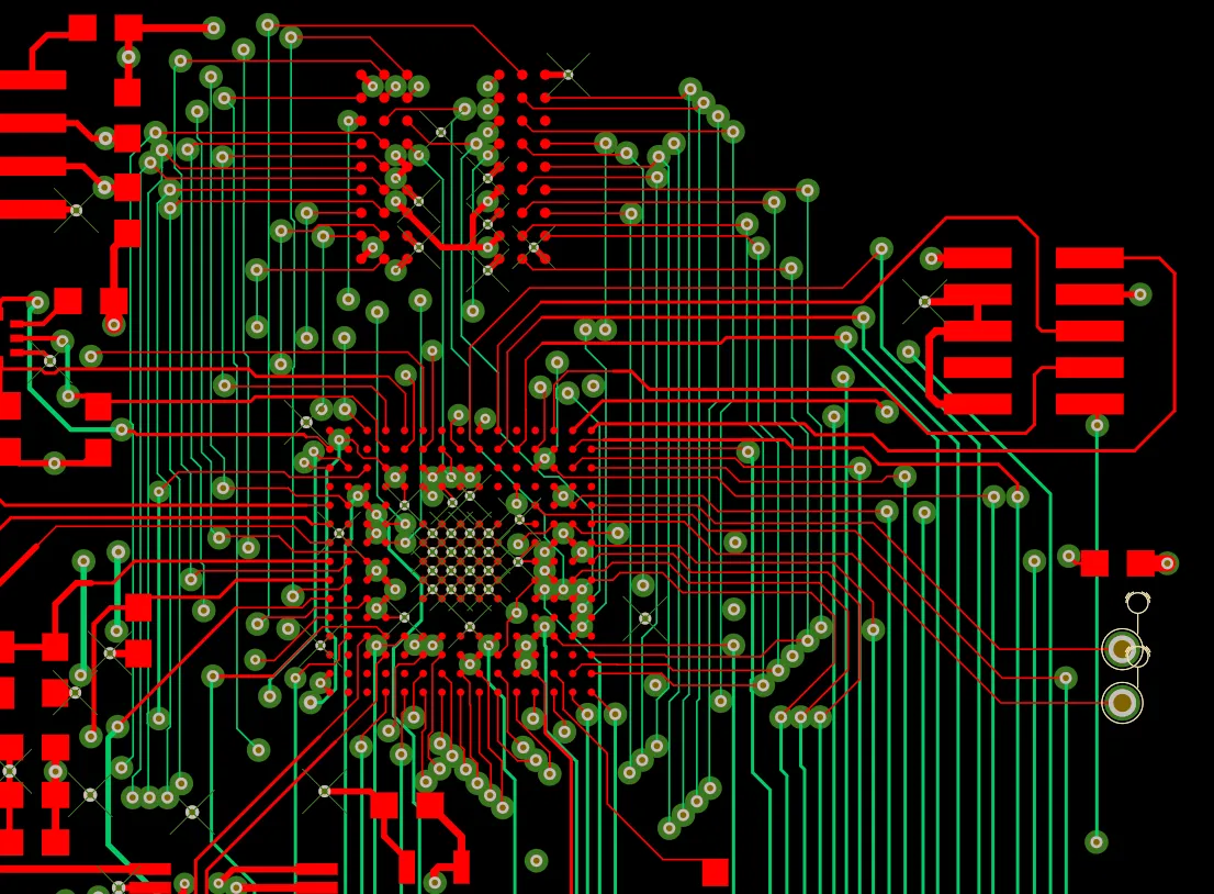
Solder mask is a thin polymer layer applied to the surface of a PCB to protect copper traces from oxidation and prevent solder from bridging between conductive areas during assembly. In a 4-layer PCB, which typically consists of two signal layers and two internal planes for power and ground, the solder mask must cover complex trace patterns and vias while leaving pads exposed for component attachment. Its primary functions include insulation, environmental protection, and defining solderable areas.
For 4-layer PCBs, solder mask design directly impacts reliability and manufacturability. Poorly designed masks can lead to solder bridges, insufficient clearance, or weak solder joints, compromising the board's performance. Moreover, manufacturability suffers if the design overlooks standard fabrication tolerances, leading to production delays or defects. A precise 4-layer PCB solder mask ensures consistent assembly outcomes, reduces rework, and enhances the board's ability to withstand thermal and mechanical stresses during operation.
Suggested Reading: Understanding Solder Mask: A Beginner's Guide to PCB Protection
Technical Principles of 4-Layer PCB Solder Mask Design
Role of Clearance in Solder Mask Design
Clearance refers to the spacing between the edge of a copper pad and the surrounding solder mask opening. In 4-layer PCB solder mask clearance, this spacing is critical to prevent solder from flowing onto adjacent areas during reflow. Insufficient clearance can cause solder bridges, while excessive clearance may expose unnecessary copper, increasing the risk of oxidation or shorts. Industry standards, such as IPC-7351B, provide guidelines for appropriate clearance values based on pad sizes and component types to ensure reliable solder joint formation.
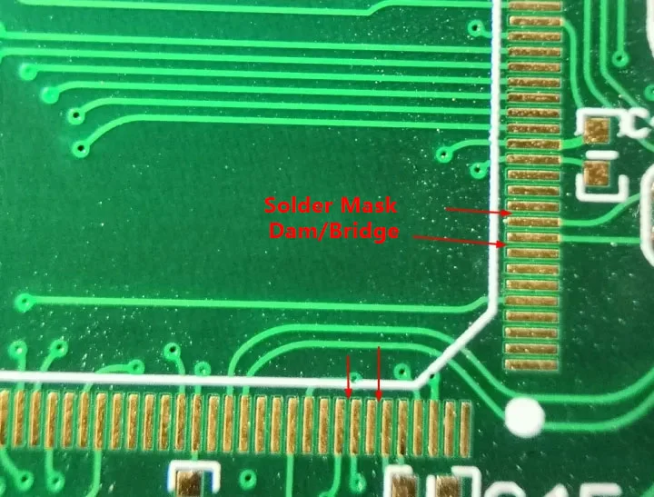
Importance of Solder Mask Dams
A 4-layer PCB solder mask dam is a narrow strip of solder mask material placed between closely spaced pads, particularly in fine-pitch components. Its purpose is to act as a barrier, preventing solder from flowing between pads and causing shorts. The width of the dam must align with fabrication capabilities, as overly thin dams may not hold during manufacturing. Standards like IPC-SM-782A offer recommendations on minimum dam widths to balance reliability and producibility.
Application Techniques and Material Properties
The 4-layer PCB solder mask application process involves coating the board with a liquid or dry film mask, exposing it to define openings, and curing it to harden the layer. The choice of material, often epoxy-based, affects the mask's thermal resistance and adhesion. Materials must withstand reflow temperatures and environmental stresses without cracking or delaminating. Adhering to specifications in IPC-SM-840E ensures that the solder mask meets performance criteria for durability and insulation.
Impact on Solder Joint Reliability
Solder joint reliability in 4-layer PCBs hinges on how well the solder mask defines the solderable area. A poorly aligned mask can lead to uneven solder distribution, creating weak joints prone to failure under thermal cycling or mechanical stress. Standards such as IPC J-STD-001H emphasize the need for precise mask openings to achieve consistent wetting and bonding during soldering, directly influencing 4-layer PCB solder joint reliability.
Practical Solutions for Optimizing 4-Layer PCB Solder Mask Design
Defining Appropriate Clearance Values
To optimize 4-layer PCB solder mask clearance, engineers should follow guidelines from IPC-7351B, which suggest a clearance of 0.05 to 0.1 millimeters around pads, depending on the component type and soldering process. This spacing accommodates manufacturing tolerances and ensures proper solder flow. During design, use PCB layout tools to verify clearance against design rules, preventing issues before fabrication begins.
Implementing Effective Solder Mask Dams
When designing a 4-layer PCB solder mask dam, ensure the dam width complies with IPC-SM-782A recommendations, typically a minimum of 0.1 millimeters for standard processes. For fine-pitch components, consult with fabrication partners to confirm achievable dimensions. Place dams strategically between pads where solder bridging risks are high, enhancing overall board reliability.
Selecting Suitable Materials and Application Methods
Choosing the right solder mask material involves evaluating its thermal and chemical resistance as per IPC-SM-840E. Liquid photoimageable masks offer precision for complex 4-layer PCB designs, while dry film masks suit simpler layouts. During application, maintain uniform thickness to avoid weak spots. Curing processes should follow manufacturer guidelines to prevent incomplete hardening, which could compromise insulation.
Enhancing Solder Joint Reliability
To improve 4-layer PCB solder joint reliability, align mask openings precisely with pad dimensions. Oversized openings can expose excess copper, while undersized ones restrict solder flow. Follow IPC J-STD-001H for soldering criteria, ensuring that mask edges do not interfere with fillet formation. Additionally, conduct thermal cycling tests post-assembly to validate joint integrity under operating conditions.
Design for Manufacturability Considerations
Incorporate design for manufacturability principles by aligning solder mask design with fabrication capabilities. Avoid overly intricate mask patterns that exceed standard process limits. Use IPC-6012E guidelines to ensure that the design supports consistent production outcomes. Verify mask alignment with copper layers to prevent registration errors, which can affect both reliability and assembly efficiency.
Troubleshooting Common Solder Mask Issues in 4-Layer PCBs
Solder mask defects can undermine the performance of 4-layer PCBs. Misalignment during application may expose unintended copper areas, risking shorts. To address this, implement strict registration checks during fabrication, guided by IPC-A-600K standards for acceptability. Another common issue is insufficient adhesion, leading to peeling under thermal stress. Ensure curing processes meet IPC-SM-840E specifications to enhance bonding. For fine-pitch designs, solder bridging due to inadequate 4-layer PCB solder mask dams is frequent. Review dam placement and width against IPC-SM-782A to mitigate this risk. Regular inspection at each manufacturing stage helps identify and correct issues early, preserving reliability.
Conclusion
Optimizing solder mask design for 4-layer PCBs is a fundamental step toward achieving superior reliability and manufacturability. By focusing on precise 4-layer PCB solder mask clearance, effective dam structures, and robust application techniques, engineers can minimize risks of defects and ensure consistent performance. Adherence to industry standards like IPC-7351B, IPC-SM-782A, and IPC J-STD-001H provides a solid foundation for creating designs that withstand operational stresses. Implementing best practices in material selection and design verification further enhances 4-layer PCB solder joint reliability. As multilayer boards continue to power complex applications, a meticulous approach to solder mask design remains indispensable for electrical engineers aiming to deliver high-quality, dependable products.
FAQs
Q1: How does 4-layer PCB solder mask clearance affect assembly quality?
A1: Clearance in 4-layer PCB solder mask design defines the space around pads for soldering. As per IPC-7351B, appropriate clearance prevents solder bridges and ensures proper fillet formation. Incorrect spacing can lead to shorts or weak joints, degrading assembly quality. Engineers must verify clearance values in layouts to align with fabrication tolerances and soldering needs.
Q2: What is the role of a 4-layer PCB solder mask dam in preventing defects?
A2: A 4-layer PCB solder mask dam acts as a barrier between closely spaced pads to stop solder bridging. Following IPC-SM-782A, a minimum dam width ensures effectiveness. Without proper dams, fine-pitch components risk shorts during reflow. Strategic dam placement is crucial for maintaining board reliability in dense designs.
Q3: Why is 4-layer PCB solder joint reliability critical for performance?
A3: 4-layer PCB solder joint reliability determines how well connections endure thermal and mechanical stress. Per IPC J-STD-001H, precise solder mask openings ensure even solder distribution for strong joints. Weak joints can fail under stress, causing circuit issues. Reliable joints are essential for consistent performance in demanding applications.
Q4: What standards guide 4-layer PCB solder mask application processes?
A4: Standards like IPC-SM-840E govern 4-layer PCB solder mask application by defining material and performance requirements. IPC-A-600K outlines acceptability criteria for finished boards. These guidelines ensure masks provide insulation and durability. Adhering to them helps achieve uniform application and long-term board protection.
References
IPC-7351B — Generic Requirements for Surface Mount Design and Land Pattern Standard. IPC, 2010.
IPC-SM-782A — Surface Mount Design and Land Pattern Standard. IPC, 1996.
IPC-SM-840E — Qualification and Performance of Permanent Solder Mask and Flexible Cover Materials. IPC, 2010.
IPC J-STD-001H — Requirements for Soldered Electrical and Electronic Assemblies. IPC, 2021.
IPC-6012E — Qualification and Performance Specification for Rigid Printed Boards. IPC, 2020.
IPC-A-600K — Acceptability of Printed Boards. IPC, 2020.