Introduction
Mixed-signal printed circuit boards integrate analog and digital circuitry on the same board, enabling compact designs for applications like data converters, sensors, and communication modules. These boards face unique noise challenges because fast digital switching can corrupt sensitive analog signals, leading to performance degradation. Electrical engineers must address noise sources in mixed-signal PCBs early in the design phase to ensure reliable operation. This guide explores key noise mechanisms and proven strategies for mixed-signal PCB noise reduction. By following structured layout practices, engineers can minimize interference and maintain signal integrity. Understanding these principles allows for robust designs that meet demanding specifications.
Understanding Noise Sources in Mixed-Signal PCBs
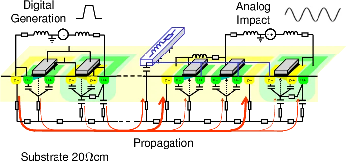
Noise in mixed-signal PCBs arises primarily from digital sections coupling into analog paths through various mechanisms. Crosstalk occurs when electromagnetic fields from adjacent traces induce unwanted voltages, especially at high frequencies where digital edges contain harmonics. Ground bounce happens during simultaneous switching of multiple digital outputs, causing voltage fluctuations on the ground plane that propagate to analog grounds. Power supply noise, generated by switching regulators or clock drivers, ripples through shared supplies and couples capacitively or inductively to signals.
External electromagnetic interference enters via board edges or cables, exacerbating internal issues. Clock signals, with their sharp transitions, radiate broadband noise that sensitive analog circuits like amplifiers pick up easily. Return path discontinuities, such as slots in ground planes, create inductive loops that amplify common-mode currents. Identifying these noise sources in mixed-signal PCBs is crucial, as even low-level interference can reduce dynamic range in ADCs or increase distortion in DACs.
Engineers often overlook radiated emissions from digital traces that reflect back and couple to analog inputs. Thermal noise from resistors and shot noise in semiconductors add intrinsic limits, but extrinsic digital noise dominates in poor layouts. Proper characterization using spectrum analyzers reveals dominant frequencies, guiding targeted mitigation.
Why Noise Control Matters in Mixed-Signal Designs
Uncontrolled noise directly impacts key metrics like signal-to-noise ratio, total harmonic distortion, and effective number of bits in converters. In precision instrumentation, even millivolt-level noise can invalidate measurements, while in RF systems, it raises noise floors and desensitizes receivers. Compliance with electromagnetic compatibility requirements becomes challenging, potentially requiring costly redesigns or shielding enclosures. Mixed-signal PCB noise reduction ensures products pass regulatory tests and perform reliably in noisy environments like automotive or industrial settings.
From a design perspective, noise margins dictate component selection and layout complexity. High noise levels force over-spec'd components, inflating costs and power consumption. As per IPC-2221C guidelines, maintaining adequate spacing between conductors helps prevent capacitive coupling, preserving margins. Ultimately, effective noise management enhances yield during manufacturing and extends field life.
Key Strategies for Partitioning and Grounding
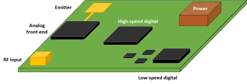
Effective mixed-signal PCB noise reduction starts with physical partitioning of analog and digital sections. Place sensitive analog components away from digital ICs, routing analog traces along dedicated paths with minimal crossings. Use split ground planes where analog and digital sections meet at a single point, often under the ADC or interface chip, to avoid ground loops. A continuous ground plane under the entire board can work if currents are managed carefully, but splits reduce coupling in most cases.
Power distribution requires separate rails for analog and digital domains, decoupled at the point of load. Local decoupling capacitors, placed within millimeters of pins, bypass high-frequency noise to ground. Ferrite beads on digital supplies isolate low-frequency bulk capacitance from analog paths. Star-point connections for grounds minimize shared impedance.
Guard traces or rings around analog areas shunt stray fields to ground, acting as electrostatic shields. Via stitching along partition boundaries lowers inductance and contains fields. These techniques align with structured engineering practices for signal isolation.
Filtering Techniques for Mixed-Signal Circuits
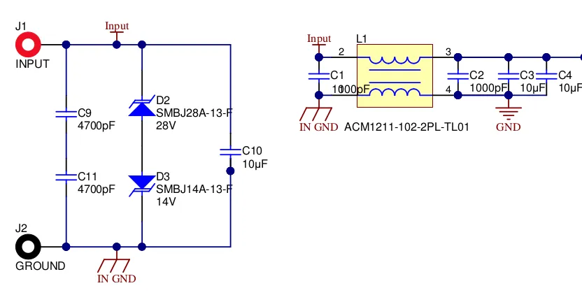
Filtering techniques for mixed-signal circuits target specific noise frequencies effectively. Pi-filters, consisting of series inductors and shunt capacitors, attenuate broadband noise on power lines entering analog sections. RC low-pass filters on signal lines smooth digital edges without excessive phase shift. For clock lines driving ADCs, series resistors dampen ringing and reduce overshoot.
Active filters using op-amps provide sharp cutoffs for narrowband interferers, but passive networks suffice for most PCB-level noise. Placement near noise sources prevents propagation, with values chosen based on cutoff frequency and impedance. Common pitfalls include inadequate damping, leading to resonances, so simulate filter response early.
In high-speed designs, IPC-2141A recommends controlled impedance for filter traces to avoid reflections. Multistage filters cascade attenuation for superior rejection. These methods integrate seamlessly into layouts, enhancing overall noise performance.
Shielding Methods for Noise Control
Shielding methods for noise control enclose sensitive areas to block electric and magnetic fields. Copper pours or cans over analog ICs reflect EMI, grounded at multiple points for low impedance. Board-level shielding uses metal frames or lids, sealed with gaskets for broadband effectiveness. Internal shielding via multi-layer stacks dedicates planes as shields between signal layers.
Guard vias fence traces, creating Faraday cages along paths. For magnetic noise, mu-metal foils near inductors offer high permeability paths. Effectiveness depends on enclosure integrity and aperture minimization. Combine with absorption materials like ferrites for hybrid control.
As outlined in IPC-2221C, plane spacing influences shielding efficacy by reducing slot antennas. These approaches scale from prototypes to production, balancing cost and performance.
Role of Common Mode Chokes in Mixed-Signal PCBs
A common mode choke in mixed signal PCB targets balanced noise on differential pairs or power lines. These inductors present high impedance to common-mode currents while allowing differential signals to pass unimpeded. Placed at board entries or between domains, they suppress conducted EMI from external cables. Surface-mount types integrate easily, with core materials selected for frequency range.
In USB or Ethernet interfaces common in mixed-signal boards, chokes prevent ground currents from digital ports reaching analog grounds. Pair with Y-capacitors across lines for capacitive filtering. Saturation current must exceed peak loads to avoid distortion. Testing involves injecting common-mode noise and measuring rejection.
Proper footprint design per IPC-2141A ensures impedance control. Chokes complement other techniques, providing 20-40 dB attenuation typically.
Troubleshooting Common Noise Issues
When noise persists, systematic debugging isolates sources. Scope analog outputs with digital off to baseline intrinsic noise, then enable sections sequentially. Near-field probes pinpoint coupling paths, revealing hotspots. FFT analysis identifies harmonics matching clock rates.
Layout reviews check for unbroken returns and via flooding. Simulation tools model parasitics pre-prototype. Manufacturing variations like plating thickness affect impedance, so validate coupons. Iterative fixes refine designs efficiently.
Conclusion
Overcoming noise in mixed-signal PCBs demands a holistic approach from partitioning to filtering and shielding. Addressing noise sources in mixed-signal PCBs through proven techniques like ground splits, pi-filters, and common mode chokes ensures high performance. Electrical engineers benefit from adhering to standards like IPC-2221C for reliable outcomes. Implementing these practices reduces iterations and enhances product quality. Prioritize simulation and measurement for optimal results. With disciplined design, mixed-signal boards achieve low noise floors and robust operation.
FAQs
Q1: What are the primary noise sources in mixed-signal PCBs?
A1: Noise sources in mixed-signal PCBs include crosstalk from parallel traces, ground bounce from simultaneous switching, and power supply ripple. External EMI and clock harmonics also contribute significantly. Partitioning analog and digital sections early mitigates these issues effectively. Proper grounding prevents loop currents from amplifying noise.
Q2: How do filtering techniques for mixed-signal circuits improve performance?
A2: Filtering techniques for mixed-signal circuits use RC or LC networks to attenuate high-frequency noise on signals and supplies. Pi-filters near ICs provide sharp roll-off without loading sources. Select components for desired bandwidth to avoid resonances. These methods boost SNR by 10-20 dB in typical designs.
Q3: What shielding methods for noise control are most effective on PCBs?
A3: Shielding methods for noise control include copper cans over analog chips and via fences along traces. Grounded pours block electric fields, while ferrites absorb magnetic noise. Multi-layer shields between planes offer broad protection. Combine with minimal apertures for optimal EMI rejection.
Q4: When should you use a common mode choke in mixed signal PCB layouts?
A4: Use a common mode choke in mixed signal PCB on power entries and differential interfaces to block balanced noise. It excels against conducted EMI from cables without affecting signals. Position near board edges and size for current handling. This technique isolates domains reliably.
References
IPC-2221C — Generic Standard on Printed Board Design. IPC, 2023
IPC-2141A — Design Guide for High-Speed Controlled Impedance Circuit Boards. IPC, 2004


