Introduction
In modern PCB design, achieving reliable high-speed signal performance demands careful attention to both pad-to-pad spacing and impedance control. Pad-to-pad spacing ensures manufacturability and prevents issues like solder bridging, while controlled impedance PCBs maintain signal integrity by minimizing distortions. These two elements form a symbiotic relationship, as improper spacing between pads can introduce crosstalk or discontinuities that disrupt impedance profiles. Engineers must balance dense layouts with precise calculations to optimize both factors. This article explores their interplay, offering structured insights for electric engineers designing next-generation boards.
Understanding Pad-to-Pad Spacing
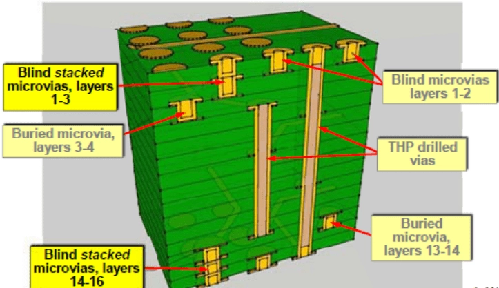
Pad-to-pad spacing refers to the minimum edge-to-edge distance between adjacent copper pads on the same layer of a PCB. This parameter is critical during fabrication and assembly to avoid short circuits from solder flow or manufacturing tolerances. In high-density interconnects, reducing spacing enables smaller footprints but increases risks of bridging, especially with fine-pitch components. Proper spacing also supports electrical isolation, aligning with voltage clearance requirements in standards like IPC-2221. Engineers evaluate it alongside trace routing to ensure overall layout feasibility.
Beyond manufacturing, pad spacing influences signal paths connecting to components. Tight spacing can force traces into proximity, amplifying coupling effects. Conversely, excessive spacing may complicate routing for controlled impedance traces. Designers use design rules to set minimums based on process capabilities, typically balancing density with reliability.
The Fundamentals of Impedance Control
Controlled impedance PCBs feature traces engineered to a specific characteristic impedance, typically 50 ohms for single-ended or 100 ohms differential, to match source and load characteristics. Impedance arises from the interaction of inductance and capacitance along the transmission line formed by the trace, dielectric, and reference planes. Variations in geometry lead to mismatches, causing reflections that degrade signals at high frequencies. Impedance control becomes essential above a few hundred MHz, where wavelengths approach trace lengths.
Key factors include trace width, dielectric thickness, and spacing to ground planes or adjacent signals. Manufacturers verify impedance through test coupons during production. For electric engineers, specifying tolerances, often ±10%, ensures consistency across the board.
The Symbiotic Link Between Pad Spacing and Impedance
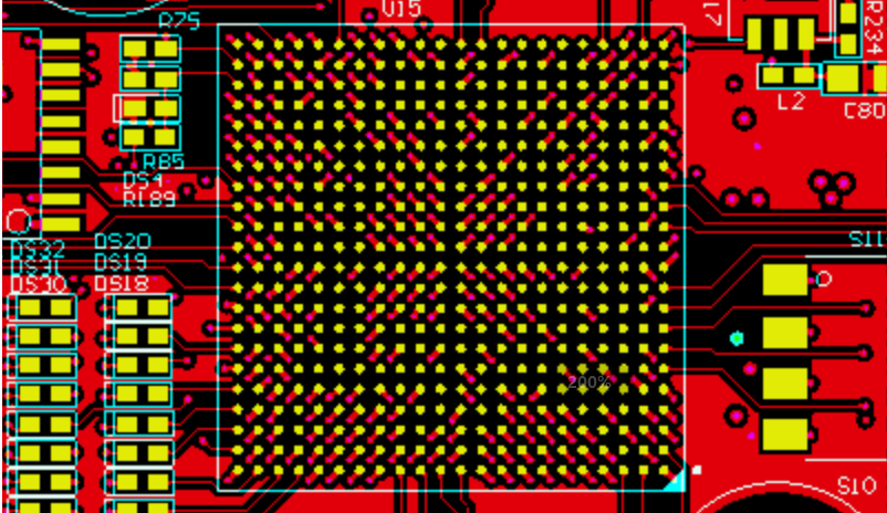
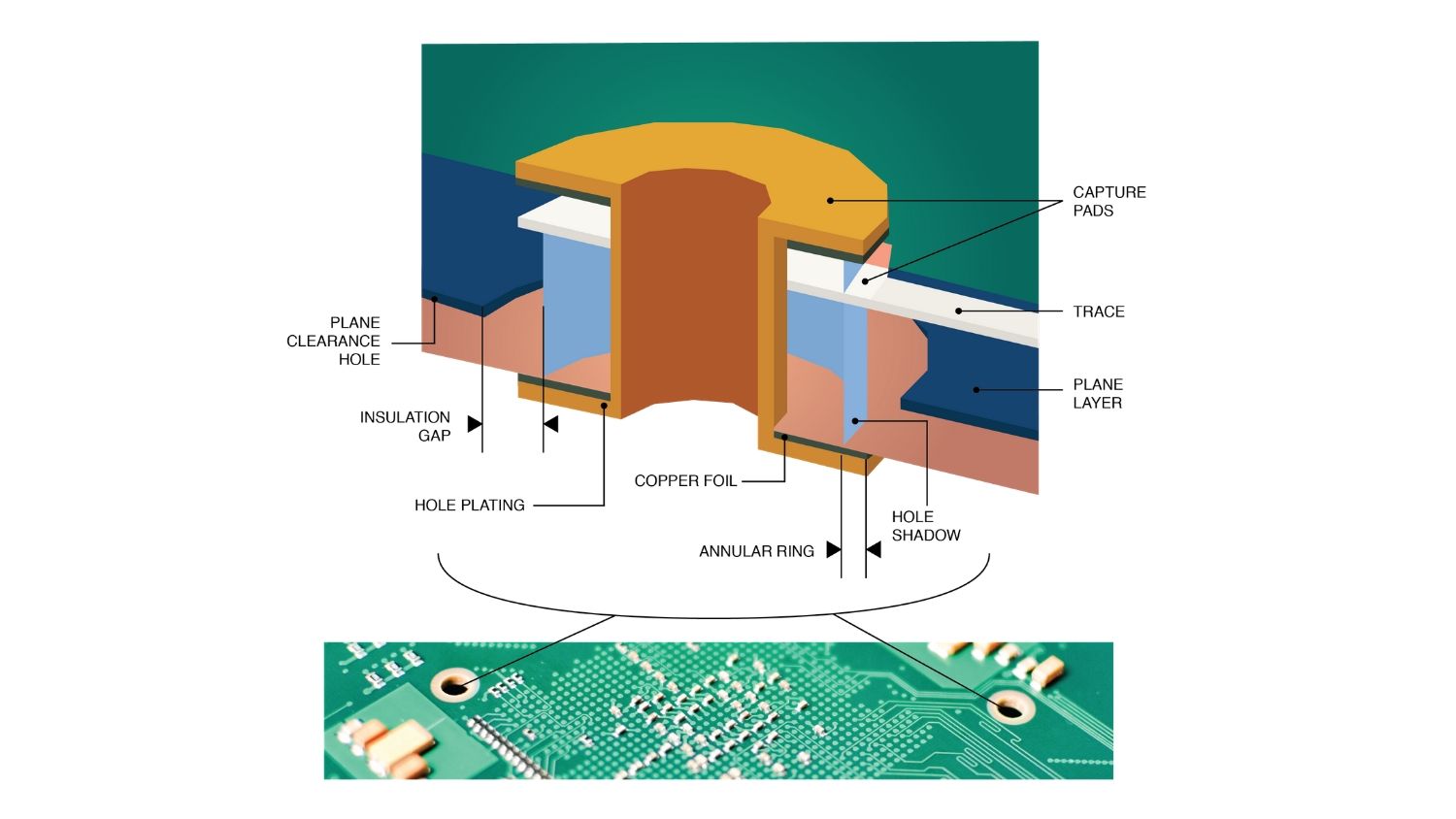
Pad-to-pad spacing and impedance control interdependent because pads anchor traces in the signal path, and their arrangement affects local field distributions. Close pad proximity can induce capacitive coupling, altering effective trace impedance near terminations. In differential pairs, pad spacing must align with intra-pair trace separation to preserve differential pair impedance. This relationship demands integrated design rules where trace width spacing calculation incorporates pad geometries.
Disruptions occur when pads encroach on controlled zones, creating stubs or widened areas that mismatch impedance. Optimal designs maintain uniform spacing from pad fanout through routing, minimizing transitions. IPC-7351 guidelines for land patterns help standardize pad sizes and spacings, supporting impedance stability. Engineers thus treat pad layout as an extension of the transmission line model.
Technical Principles of Impedance in PCB Traces
Transmission line theory governs impedance, with characteristic impedance Z0 approximated as Z0 = (87 / sqrt(Er + 1.41)) * ln(5.98h / (0.8w + t)) for microstrips, where geometry dictates L and C per unit length. Trace width directly impacts capacitance to plane, while spacing to adjacent traces controls mutual inductance. In stripline configurations, symmetric spacing to dual planes simplifies control but requires precise etching.
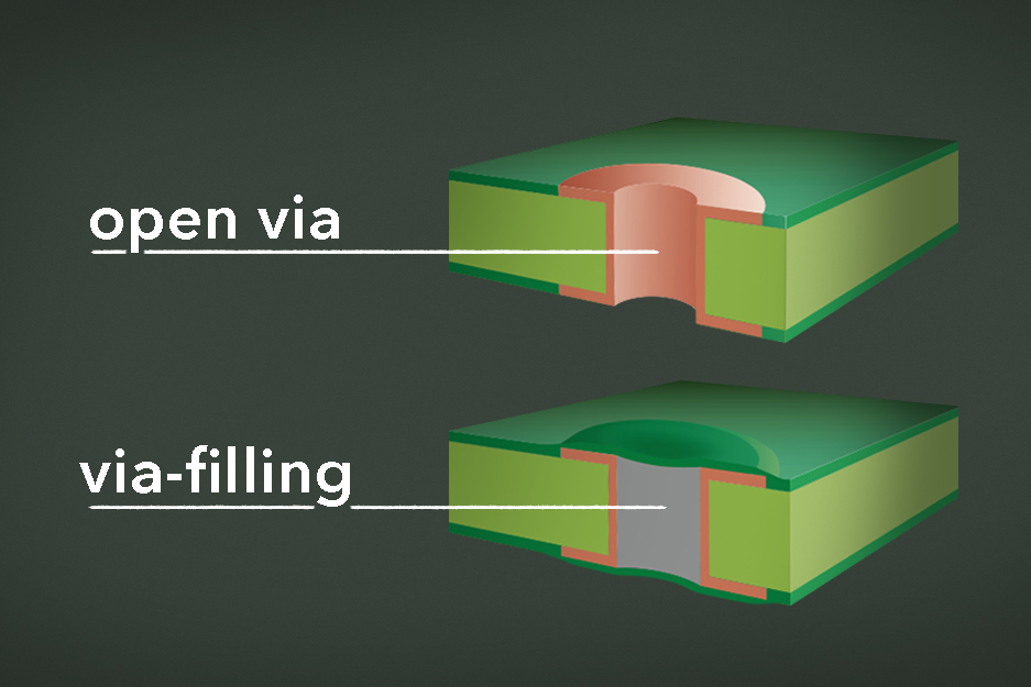
For high-speed signals, signal reflection minimization relies on impedance continuity. Reflections coefficient Gamma = (Zload - Z0)/(Zload + Z0) quantifies mismatches, leading to ringing or attenuation. Pad areas introduce higher capacitance due to larger copper, necessitating tapered fanouts or stitching vias for return paths.
Trace Width Spacing Calculation for Controlled Impedance
Trace width spacing calculation starts with stackup definition, including dielectric constants and thicknesses. Field-solving software models the structure to iterate widths and spacings for target Z0. Single-ended traces prioritize width for Z0, with edge-to-edge spacing at least 3 times width to curb crosstalk. Engineers input material Er, copper weight, and plane proximity to generate tables.
In practice, fabrication tolerances affect outcomes, so coupons validate post-etch measurements using TDR. Adjustments account for etch factor, where inner layers need wider traces. This process ensures controlled impedance PCB performance across frequencies.
Differential Pair Impedance and Spacing Dynamics
Differential pair impedance focuses on two traces carrying balanced signals, with Zdiff = 2 * Z0 * (1 - k), where k is coupling coefficient influenced by edge spacing. Tight intra-pair spacing enhances coupling, lowering Zdiff, ideal for 90-100 ohm targets in LVDS or PCIe. Inter-pair spacing, akin to pad-to-pad in fanout regions, prevents mode conversion or skew.
Maintaining constant spacing avoids intra-pair imbalance, critical for common-mode rejection. Pad spacing for differential pins must mirror trace geometry to extend controlled coupling. Variations introduce reflections, undermining eye diagrams.
Impedance Matching Techniques in Dense Layouts
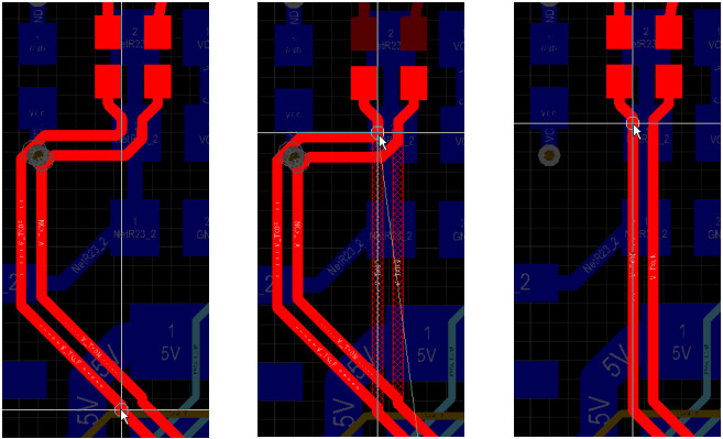
Impedance matching techniques include serpentine length tuning for delay skew and back-drilling vias to remove stubs. Consistent dielectric stacking preserves Z0 across layers. For pad transitions, dog-bone fanouts widen gradually to match trace width without abrupt changes.
Routing high-speed nets first reserves space, integrating pad spacing rules early. Ground plane cutouts under pads minimize parasitic capacitance. These methods synergize with pad spacing to achieve uniform impedance profiles.
Best Practices for Integration
Establish design rules linking pad spacing minima to impedance targets, using 3W rule for non-critical spacing. Simulate full nets including pads for discontinuity analysis. Collaborate with fabricators for stackup trade-offs, specifying impedance tolerances.
Verify with TDR on prototypes, correlating to pad regions. Reference J-STD-001 for assembly impacts on spacing integrity. These practices yield robust controlled impedance PCBs.
Troubleshooting Common Issues
Engineers often encounter impedance bumps near pads due to oversized lands or asymmetric fanouts. Crosstalk spikes from violated pad-to-pad minima manifest as eye closure. Reflections from spacing violations show in time-domain reflectometry.
Mitigate by refining land patterns per standards and rerouting pairs. Post-layout extraction models confirm fixes before fab.
Conclusion
Pad-to-pad spacing and impedance control share a vital symbiosis in PCB design, where spacing governs both manufacturability and signal fidelity. Logical integration through stackup planning, precise calculations, and verification ensures high-performance boards. Electric engineers leveraging these principles minimize signal reflection and maximize density. Adopting best practices aligned with industry standards delivers reliable outcomes in demanding applications.
FAQs
Q1: How does trace width spacing calculation impact controlled impedance PCB design?
A1: Trace width spacing calculation determines geometry for target Z0 by balancing capacitance and inductance. Wider traces lower impedance but demand greater spacing to adjacent signals, preventing crosstalk. Engineers iterate using stackup parameters, ensuring tolerances meet fab capabilities. This process directly supports signal reflection minimization in high-speed nets.
Q2: What role does pad spacing play in differential pair impedance?
A2: Pad spacing in differential pairs must match intra-pair trace separation to maintain consistent coupling and Zdiff. Deviations introduce discontinuities, degrading balance and increasing EMI. Aligning pad-to-pad distances with routing rules preserves impedance profile from component to via. This integration is key for applications like USB or Ethernet.
Q3: What are effective impedance matching techniques for minimizing reflections?
A3: Impedance matching techniques include uniform trace geometries, optimized via transitions, and reference plane continuity. Tapered fanouts from pads reduce capacitive loading, while consistent spacing avoids mismatches. Pre-layout simulations guide adjustments, ensuring Z0 alignment across the board. These steps effectively minimize signal reflections in controlled impedance designs.
Q4: Why is pad-to-pad spacing critical for signal reflection minimization?
A4: Pad-to-pad spacing prevents excessive coupling that alters local impedance, a primary cause of reflections. Adequate clearance maintains trace isolation, supporting overall Z0 control. In dense layouts, it enables precise trace width spacing calculation without compromises. Proper enforcement aligns with high-speed integrity goals.
References
IPC-2221B — Generic Standard on Printed Board Design. IPC, 2012
IPC-7351B — Generic Requirements for Surface Mount Design and Land Pattern Standard. IPC, 2010
J-STD-001G — Requirements for Soldered Electrical and Electronic Assemblies. IPC, 2011