Introduction
Printed Circuit Board assembly cost remains a critical concern for electrical engineers striving to balance quality and budget in electronics manufacturing. The expenses tied to assembling a PCB can significantly impact the overall project cost, especially in high volume production. Factors such as board shape, thermal management techniques like thermal relief, and trace routing methods play substantial roles in determining these costs. Understanding and optimizing these elements can lead to substantial savings without compromising performance. This article explores the key drivers behind PCB assembly cost and offers practical strategies for electrical engineers to minimize expenses while maintaining reliability. By focusing on design choices and manufacturing considerations, engineers can achieve cost effective solutions tailored to their specific needs.
What Is PCB Assembly Cost and Why It Matters
PCB assembly cost refers to the total expenditure involved in mounting components onto a printed circuit board to create a functional electronic assembly. This includes labor, materials, equipment, and overheads associated with the process. For electrical engineers, managing these costs is vital as they directly influence product pricing and profitability. High assembly costs can render a project unfeasible, particularly in competitive markets where margins are thin. Beyond financial implications, assembly cost also affects production timelines and scalability. Inefficient designs or complex board shapes can increase manufacturing time and error rates, leading to rework and delays. By prioritizing cost optimization during the design phase, engineers ensure smoother production runs and better alignment with project goals, making cost management an integral part of successful PCB development.
Suggested Reading: PCB Cost Calculator: How PCB and Assembly Pricing Is Estimated
Key Factors Influencing PCB Assembly Cost
Several technical and design factors contribute to the overall cost of PCB assembly. Understanding these elements allows engineers to make informed decisions during the design and production stages. Below are the primary drivers that impact expenses in this process.
Board Shape and Complexity
The shape of a PCB significantly affects assembly costs. Engineers should stick to regular board shapes, such as rectangles or squares, to minimize manufacturing expenses. These standard geometries align well with automated assembly equipment, reducing setup time and material waste. Irregular shapes or custom outlines often require specialized tooling or manual handling, which increases labor costs and production time. Additionally, non standard shapes can complicate panelization, the process of arranging multiple boards on a single panel for efficient manufacturing. Poor panel utilization leads to higher material costs. By adhering to simple, regular shapes like rectangles or squares, engineers can streamline the assembly process and achieve notable cost reductions.
Component Placement and Density
The arrangement and density of components on a PCB directly influence assembly costs. Dense layouts may require advanced pick and place machines or additional inspection steps to ensure accuracy, driving up expenses. Conversely, overly sparse designs can waste board space, increasing material costs. Engineers must balance component placement to optimize both space and assembly efficiency. Grouping similar components together can reduce machine reprogramming time during assembly. Additionally, ensuring adequate spacing between components prevents soldering defects and simplifies rework if needed. Following industry guidelines for component placement can help maintain cost efficiency while upholding assembly quality.
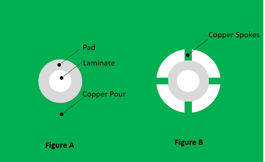
Thermal Management and Thermal Relief
Thermal management is a crucial consideration in PCB design, impacting both performance and assembly cost. Incorporating thermal relief, a technique involving specific pad designs to manage heat dissipation during soldering, can prevent issues like component damage or board warpage. Thermal relief patterns, typically spoke like connections between pads and copper planes, reduce heat transfer to surrounding areas, easing the soldering process. Without proper thermal relief, excessive heat can lead to inconsistent solder joints, increasing rework costs. Engineers should design pads with thermal relief in mind, especially for components connected to large ground planes, to ensure reliable soldering and lower assembly expenses.
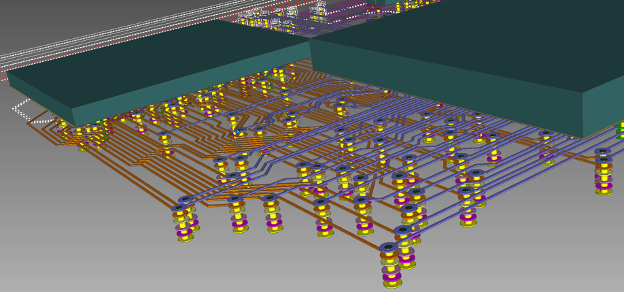
Trace Routing and Signal Integrity
Effective trace routing methods are essential for maintaining signal integrity and controlling assembly costs. Poorly routed traces can lead to signal interference, requiring additional layers or redesigns that elevate expenses. Employing effective trace routing methods, such as minimizing trace length and avoiding sharp angles, ensures reliable performance while keeping manufacturing straightforward. Engineers should prioritize direct paths for critical signals and maintain consistent trace widths to avoid impedance mismatches. Additionally, reducing via usage through efficient routing can lower drilling costs during production. By focusing on optimized trace routing, engineers can prevent costly design iterations and enhance overall assembly efficiency.
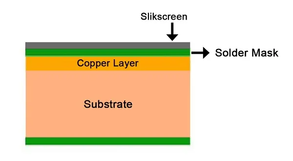
Material Selection and Layer Count
The choice of materials and the number of layers in a PCB design also affect assembly costs. High performance materials, while beneficial for specific applications, often come with higher price tags and may require specialized assembly processes. Similarly, multilayer boards increase costs due to additional fabrication steps and alignment precision needed during assembly. Engineers should evaluate whether the performance benefits justify the added expense. Opting for standard materials and minimizing layer count, where feasible, can significantly reduce costs without sacrificing functionality. Balancing material quality with budget constraints is key to cost effective assembly.
Related Reading: PCB Material Selection: Balancing Thermal Performance and Cost
Practical Strategies for Reducing PCB Assembly Cost
Electrical engineers can adopt several strategies to optimize PCB assembly costs without compromising on quality. These actionable approaches focus on design simplification and manufacturing efficiency, aligning with industry best practices.
Standardize Board Shapes for Efficiency
As emphasized earlier, sticking to regular board shapes, such as rectangles or squares, simplifies the manufacturing process. This standardization reduces setup times for cutting and panelization, lowering labor and material costs. Engineers should avoid complex outlines unless absolutely necessary for the application. When custom shapes are required, consider breaking the design into smaller, regular shaped sections that can be assembled separately. This approach maintains compatibility with automated equipment, ensuring cost efficiency throughout the assembly process.
Implement Thermal Relief Designs
Incorporating thermal relief in pad designs is a practical way to manage heat during soldering and reduce assembly issues. By using spoke patterns or reduced copper connections around pads tied to large planes, engineers can prevent excessive heat buildup that might damage components or cause soldering defects. This technique, guided by standards like IPC-2221B, helps achieve consistent solder joints and minimizes rework, directly impacting cost savings. Careful attention to thermal relief during the design phase ensures smoother assembly and enhances board reliability.
Optimize Trace Routing for Manufacturability
Employing effective trace routing methods can streamline the assembly process and reduce costs. Engineers should aim for minimal trace lengths and avoid unnecessary vias to lower drilling expenses. Maintaining consistent trace widths and spacing, as outlined in standards like IPC-2152, ensures signal integrity and prevents manufacturing errors. Additionally, routing critical signals away from noisy areas reduces the risk of interference, avoiding costly redesigns. By prioritizing clean and efficient trace routing, engineers can achieve reliable performance while keeping assembly costs in check.
Minimize Layer Count and Material Costs
Reducing the number of layers in a PCB design directly lowers fabrication and assembly costs. Engineers should assess whether additional layers are essential for the circuit’s functionality. If possible, consolidate signals onto fewer layers using efficient routing techniques. Similarly, selecting standard materials over high cost alternatives can yield savings without affecting performance for many applications. Consulting standards like IPC-6012E for material and layer specifications ensures compliance while guiding cost effective decisions during the design process.
Collaborate Early with Manufacturing Teams
Engaging with manufacturing teams during the design phase can uncover cost saving opportunities. Feedback on design for manufacturability can highlight potential assembly challenges, such as component placement or routing issues, before production begins. Early collaboration helps align the design with assembly capabilities, reducing the likelihood of errors or delays. Engineers should share design files and discuss constraints to ensure the board is optimized for efficient assembly, ultimately lowering overall costs.
Troubleshooting Common Cost Related Issues in PCB Assembly
In my experience as an assembly engineer, certain recurring issues often drive up PCB assembly costs unexpectedly. One common problem is misalignment during component placement, often due to unclear fiducial markers or irregular board shapes. This can lead to rework, increasing labor expenses. To address this, ensure fiducial markers are well defined and stick to regular board shapes, such as rectangles or squares, for better compatibility with assembly equipment. Another frequent issue is soldering defects caused by inadequate thermal relief on pads connected to large copper planes. Implementing proper thermal relief designs can mitigate heat related soldering problems, saving time and cost. Finally, inefficient trace routing can cause signal issues, necessitating redesigns. Employing effective trace routing methods early in the design process prevents such setbacks, ensuring a smoother and more cost effective assembly.
Conclusion
Managing PCB assembly cost is a multifaceted challenge for electrical engineers, requiring careful consideration of design and manufacturing factors. By focusing on regular board shapes like rectangles or squares, integrating thermal relief for better heat management, and employing effective trace routing methods, engineers can significantly reduce expenses. These strategies, combined with material optimization and early collaboration with manufacturing teams, ensure cost efficiency without compromising quality. Adhering to industry standards and prioritizing design for manufacturability further enhances assembly outcomes. Ultimately, a proactive approach to cost management during the design phase empowers engineers to deliver reliable, budget friendly PCB solutions tailored to project demands.
FAQs
Q1: How does sticking to regular board shapes, such as rectangles or squares, reduce PCB assembly cost?
A1: Sticking to regular board shapes like rectangles or squares minimizes setup time and material waste during manufacturing. These shapes align with automated assembly equipment, reducing labor costs and improving panel utilization. Irregular shapes often require custom tooling or manual handling, increasing expenses. Standard geometries streamline production, ensuring cost efficiency.
Q2: What role does thermal relief play in controlling PCB assembly expenses?
A2: Thermal relief manages heat dissipation during soldering, preventing component damage and inconsistent joints. By using spoke patterns on pads connected to copper planes, it reduces rework needs. This lowers labor costs and enhances assembly reliability, directly impacting overall expenses in a positive way.
Q3: Why should engineers employ effective trace routing methods in PCB design?
A3: Employing effective trace routing methods ensures signal integrity and reduces manufacturing errors. Short, direct traces with minimal vias lower drilling costs and prevent interference. Optimized routing avoids redesigns, saving time and money during assembly while maintaining performance, making it a critical cost saving strategy.
Q4: How can early collaboration with manufacturing teams impact PCB assembly cost?
A4: Early collaboration identifies assembly challenges before production, such as component placement issues. Feedback on design for manufacturability aligns the PCB with equipment capabilities, reducing errors and delays. This proactive approach minimizes rework and ensures a cost effective assembly process from the start.
References
IPC-2221B — Generic Standard on Printed Board Design. IPC, 2012.
IPC-2152 — Standard for Determining Current Carrying Capacity in Printed Board Design. IPC, 2009.
IPC-6012E — Qualification and Performance Specification for Rigid Printed Boards. IPC, 2020.