Introduction
In the realm of printed circuit board design, ground planes play a pivotal role in ensuring reliable performance and signal integrity. These layers, often composed of a relatively large area of copper, serve as the electrical ground reference for circuits, providing a stable foundation for electronic components. Ground planes are critical for shielding sensitive signals from interference, managing thermal distribution, and reducing electromagnetic noise in high speed designs. For electrical engineers, understanding the functionality and implementation of ground planes is essential to creating robust and efficient circuit boards. This article explores the fundamental concepts behind ground planes, their importance in modern electronics, and best practices for incorporating them into designs. The focus will be on their role in shielding, thermal management, and maintaining a low impedance return path.
What Are PCB Ground Planes?
A PCB ground plane is a continuous layer of copper on a printed circuit board that acts as a common electrical ground reference for all components and signals. Typically covering a relatively large area of copper, it provides a low impedance path for return currents, ensuring that signals maintain their integrity across the board. Ground planes are often found in multilayer PCBs, where they occupy an entire layer or a significant portion of it, positioned strategically to support signal and power layers.
The primary purpose of a ground plane is to establish a uniform reference voltage, minimizing voltage drops and noise in the circuit. Beyond this, ground planes contribute to shielding by reducing electromagnetic interference between adjacent traces and components. They also assist in thermal management by distributing heat across the board, especially when thermals are placed to connect components to the plane. Their presence is vital in high frequency and high speed designs, where signal stability is paramount.
Technical Principles of Ground Planes
Electrical Ground and Return Path
The core function of a ground plane is to serve as the electrical ground, offering a reference point for all voltages in the circuit. In any electronic system, current must return to its source, and a ground plane ensures this happens via the shortest, lowest impedance path. A relatively large area of copper minimizes resistance and inductance, reducing voltage drops and noise that could disrupt signal integrity.
In high speed designs, the return path is especially critical. Signals traveling along traces generate electromagnetic fields, and the return current must flow directly beneath the signal trace to minimize loop area. A continuous ground plane ensures this by providing an uninterrupted path, preventing signal reflections and maintaining performance.
Shielding and Electromagnetic Interference
Ground planes are instrumental in shielding circuits from electromagnetic interference. By covering a significant portion of the board with copper, they create a Faraday cage like effect, blocking external fields from affecting sensitive traces. This shielding capability also works in reverse, containing emissions from the PCB to prevent interference with nearby devices.
For effective shielding, the ground plane must be unbroken and strategically placed near signal layers. Breaks or splits in the plane can create slots that act as antennas, radiating noise instead of suppressing it. Electrical engineers must prioritize continuity in ground plane design to maximize this protective function.
Thermal Management with Thermals
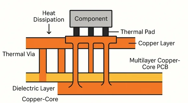
Thermal management is another key aspect of ground plane design. Components generating heat, such as power transistors or integrated circuits, can transfer excess heat to the ground plane through thermals. These are small copper connections between a component’s pad and the ground plane, designed to conduct heat away from the source.
A relatively large area of copper in the ground plane acts as a heat sink, spreading thermal energy across the board. This prevents localized hot spots that could damage components or degrade performance. Proper placement of thermals ensures efficient heat dissipation without compromising the electrical integrity of the ground connection.
Suggested Reading: Ground plane for beginners: Making your first circuit!
Best Practices for Designing Ground Planes
Ensure Continuity and Avoid Splits
One fundamental rule in ground plane design is to maintain continuity. Splits or cuts in the ground plane can disrupt return paths, leading to increased noise and signal integrity issues. If multiple ground types are necessary, such as analog and digital grounds, they should be connected at a single point to avoid creating separate planes that could introduce interference.
Optimize Layer Stackup
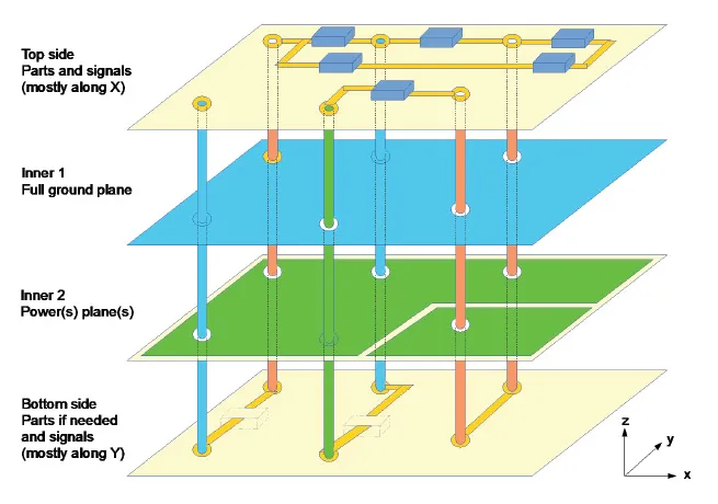
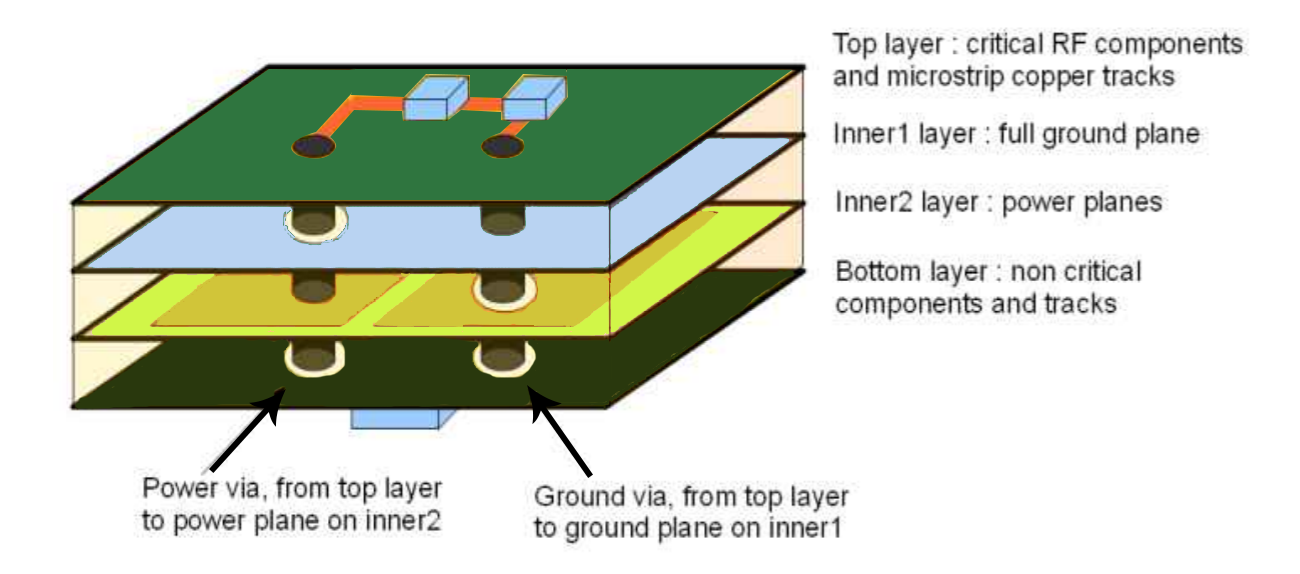
In multilayer PCBs, the placement of the ground plane within the stackup is critical. Positioning the ground plane adjacent to signal layers minimizes the loop area for return currents, enhancing signal integrity. A common stackup for a four layer board includes signal layers on the top and bottom, with ground and power planes in the middle. This configuration provides shielding and a stable reference for signals.
Use Vias for Ground Connections
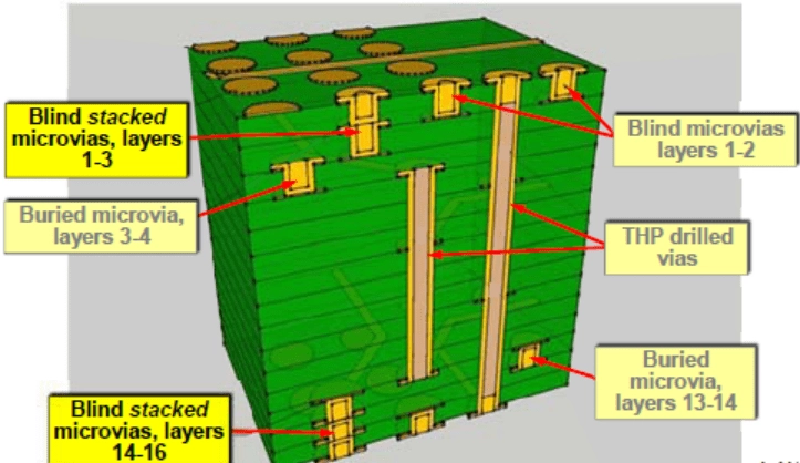
To connect components to the ground plane across different layers, vias are essential. These small conductive holes ensure a low impedance connection to the electrical ground. Placing multiple vias near high current components reduces resistance and improves performance. For high frequency designs, stitching vias around the board’s perimeter can enhance shielding by tying all ground layers together.
Incorporate Thermals for Heat Dissipation
When designing for thermal management, thermals should be added to connect heat generating components to the ground plane. The number and size of thermals depend on the component’s power dissipation and the board’s thermal requirements. Care must be taken to balance thermal conductivity with manufacturability, as excessive thermals can complicate soldering processes.
Minimize Loop Areas in High Speed Designs
For high speed circuits, minimizing the loop area between signal traces and their return paths is vital. A continuous ground plane directly beneath signal traces ensures the return current follows the shortest path, reducing inductance and electromagnetic interference. Avoid routing high speed signals over splits or gaps in the ground plane to maintain signal quality.
Common Challenges and Solutions in Ground Plane Design
Managing Ground Bounce
Ground bounce occurs when rapid switching of digital signals causes transient voltage fluctuations in the ground plane. This can disrupt signal levels and lead to errors. To mitigate ground bounce, use decoupling capacitors near integrated circuits to stabilize the voltage. Additionally, ensure the ground plane has a low impedance path by using a relatively large area of copper and multiple vias.
Balancing Thermal and Electrical Needs
A challenge in designs with thermals is balancing heat dissipation with electrical isolation. Excessive thermals can make soldering difficult by drawing heat away from the pad too quickly. A common solution is to use a spoke pattern for thermals, where narrow copper connections limit heat flow during soldering while still allowing thermal transfer during operation.
Addressing High Frequency Noise
In high frequency applications, ground planes can inadvertently act as antennas if not designed properly. Slots or breaks in the plane can radiate noise, compromising shielding. To address this, maintain a continuous ground plane and use stitching vias to connect multiple ground layers, creating a robust shield against high frequency interference.
Conclusion
PCB ground planes are a cornerstone of effective circuit board design, providing a stable electrical ground, enhancing shielding, and aiding in thermal management. By covering a relatively large area of copper, they ensure low impedance return paths, protect against electromagnetic interference, and distribute heat through strategically placed thermals. Electrical engineers must prioritize continuity, proper layer stackup, and via placement to maximize the benefits of ground planes. Understanding and implementing these principles leads to reliable, high performance designs that meet the demands of modern electronics. As technology advances, the role of ground planes will remain central to achieving signal integrity and system stability.
FAQs
Q1: What is the role of a relatively large area of copper in a PCB ground plane?
A1: A relatively large area of copper in a PCB ground plane provides a low impedance path for return currents, ensuring signal integrity. It also enhances shielding against electromagnetic interference and acts as a heat sink for thermal management. This expansive copper coverage minimizes voltage drops and noise, making it essential for stable circuit performance in complex designs.
Q2: How does a ground plane contribute to shielding in PCB designs?
A2: A ground plane contributes to shielding by forming a barrier that blocks external electromagnetic interference from affecting sensitive signals. It also contains emissions from the PCB, preventing interference with nearby devices. By maintaining a continuous copper layer, it creates a protective effect, crucial for high frequency and densely packed electronic environments.
Q3: Why are thermals important when connecting components to a ground plane?
A3: Thermals are important for connecting components to a ground plane as they facilitate heat dissipation from heat generating parts to the copper layer. They prevent localized overheating, extending component lifespan. Properly designed thermals balance thermal conductivity with ease of soldering, ensuring both electrical connection and effective thermal management in the design.
Q4: How does an electrical ground improve signal integrity in PCBs?
A4: An electrical ground, provided by a ground plane, improves signal integrity by offering a stable reference voltage and a low impedance return path for currents. This minimizes noise, crosstalk, and signal distortions, especially in high speed designs. A well implemented ground plane ensures consistent performance across the circuit, reducing the risk of data errors.
References
IPC-2221B - Generic Standard on Printed Board Design. IPC, 2012.
IPC-6012E - Qualification and Performance Specification for Rigid Printed Boards. IPC, 2020.
IPC-A-600K - Acceptability of Printed Boards. IPC, 2020.
IEC 60950-1:2005+AMD1:2009+AMD2:2013 - Information Technology Equipment - Safety - Part 1: General Requirements. IEC, 2013.