Introduction
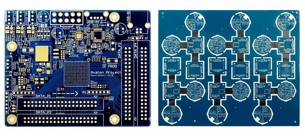
PCB panelization involves combining multiple individual circuit boards onto a single large panel to streamline manufacturing and assembly processes. This approach enhances efficiency in surface mount technology (SMT) production by allowing automated handling and processing of batches. However, PCB panel component placement plays a crucial role in ensuring high yields and minimizing defects. Improper sizing of the panel or suboptimal positioning of components can lead to issues like mechanical stress during depaneling, solder joint failures, or handling damage. Electric engineers must prioritize these factors to align design with fabrication capabilities. Understanding best practices for PCB panel size and component placement directly impacts overall production reliability.

Understanding PCB Panelization and Its Impact on Component Placement
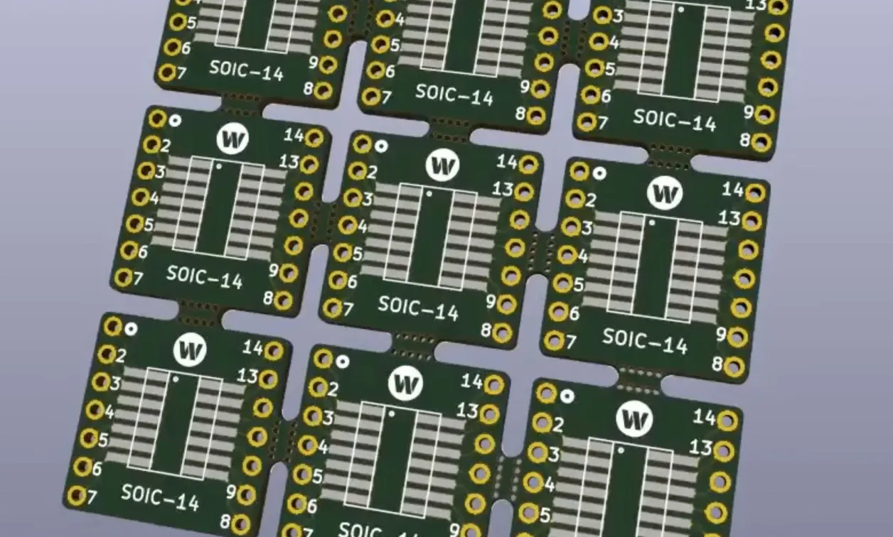
PCB panelization refers to the process of arraying several identical or varied boards on a substrate panel optimized for high-volume manufacturing. This method reduces setup times for printers, pick-and-place machines, and reflow ovens while maximizing material use. Component placement on the panel must account for the entire array's geometry to prevent interference between neighboring boards. Factors such as panel dimensions influence thermal uniformity during soldering and mechanical stability post-fabrication. Poorly planned PCB panel component placement can exacerbate warpage or expose sensitive parts to edge stresses. Engineers benefit from viewing the panel as a unified structure rather than isolated boards.
The relevance of these practices stems from their direct effect on assembly yield and cost. In SMT environments, machines process the full panel, so component orientation on PCB panel must support machine vision and motion paths. Deviations in placement can cause misalignment, tombstoning, or bridging defects. Keepout zones on PCB panel further protect critical areas from unintended overlaps. By adhering to established guidelines, teams avoid rework and ensure compliance with quality benchmarks.
Key Considerations for PCB Panel Size Selection
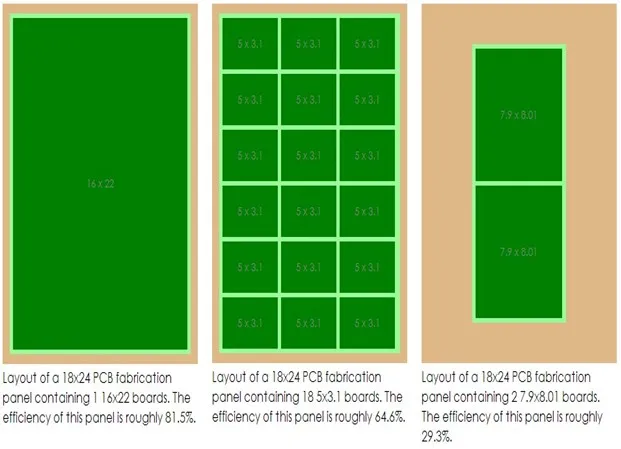
Selecting the appropriate PCB panel size balances production efficiency, equipment compatibility, and material waste. Panels too large may warp under their own weight or exceed handler limits, while undersized ones reduce throughput. Engineers should evaluate machine specifications alongside board count to optimize layout. Uniform component distribution across the panel helps mitigate thermal gradients during reflow. Aspect ratios close to standard formats promote stability in lamination and plating stages.
Panel size also influences fiducial placement for alignment. Positioning fiducials at panel corners and board peripheries ensures precise registration for SMT component placement on panelized PCB. Oversized panels demand additional supports like breakaway tabs to prevent flexing. Collaboration between design and manufacturing teams refines these choices early.
Best Practices for Component Clearance on PCB Panel
Component clearance on PCB panel is essential to safeguard parts from damage during routing, V-scoring, or milling depaneling. Maintain sufficient margins between components and panel edges or inter-board gaps to accommodate tooling stresses. This spacing prevents cracks in tall components or delamination near score lines. Engineers should define clearances based on depaneling method, with wider gaps for mechanical routing versus laser cutting.
In practice, position low-profile components nearer edges where feasible, reserving inner areas for taller parts. This strategy reduces the risk of collision during singulation. Verify clearances through design rule checks that simulate panel stresses. Consistent application across the array upholds assembly integrity.
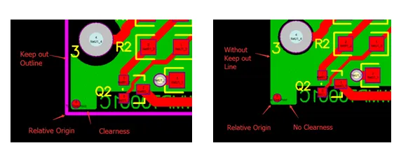
Implementing Keepout Zones on PCB Panel
Keepout zones on PCB panel designate restricted areas free from components, traces, or vias to facilitate manufacturing operations. These zones typically encircle panel borders, fiducials, and breakaway features like tabs or mouse bites. By enforcing keepouts, designers prevent solder paste extrusion or pick-and-place errors near critical boundaries. IPC-2221 provides foundational guidelines for such spatial requirements in board design.
Define keepout polygons in layout software, specifying restrictions for top, bottom, and inner layers. Extend zones beyond mechanical outlines to account for tool runout. Troubleshooting often reveals issues from overlooked keepouts, such as fiducial obstruction. Regular design reviews ensure zones align with process flows.
Optimizing Component Orientation on PCB Panel
Component orientation on PCB panel streamlines automated assembly by minimizing machine head rotations and travel distances. Align similar parts in the same direction across the array to enhance pick-and-place efficiency and reduce programming complexity. For polarized components like diodes or ICs, consistent theta angles prevent reflow shadowing where larger parts block solder on smaller ones behind them.
Consider airflow in reflow ovens by avoiding dense clusters that trap heat unevenly. Rotate boards within the panel if needed to balance mass distribution and curb warpage. IPC-A-610 outlines acceptability criteria for post-reflow placement, emphasizing orientation's role in joint quality. Test orientations via simulation to predict machine throughput.
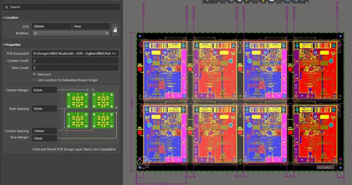
SMT Component Placement on Panelized PCB: Specialized Guidelines
SMT component placement on panelized PCB demands precision to handle array-scale tolerances. Place fiducials strategically, with global marks for panel alignment and local ones per board for fine tuning. This dual system compensates for panel stretching or contraction post-lamination. Ensure stencil apertures align perfectly across the panel to avoid uneven paste volume.
Group components by height and feeder type to optimize machine sequencing. Avoid placing fine-pitch parts near panel edges prone to vibration. J-STD-001 addresses soldering requirements that influence placement decisions on multi-board panels. Validate setups with trial runs on small arrays.
Common Challenges and Troubleshooting Tips
Uneven component density often causes panel warpage, leading to placement inaccuracies. Balance top and bottom side populations to equalize reflow stresses. Depaneling-induced microcracks near edges highlight insufficient clearances; audit zones post-prototype. Fiducial misalignment from panel flexure calls for reinforced tooling holes.
Troubleshoot orientation issues by analyzing machine logs for excessive rotations. Adjust keepouts iteratively based on yield data. These steps, grounded in standards like IPC-A-610, elevate panelized production reliability.
Conclusion
Mastering PCB panel size and component placement integrates design foresight with manufacturing realities for superior outcomes. Prioritizing clearances, keepout zones, and orientations minimizes defects in high-volume SMT runs. Electric engineers gain from structured approaches that enhance yield and scalability. Implement these best practices to optimize panelized workflows effectively.
FAQs
Q1: What are the main factors influencing PCB panel component placement?
A1: PCB panel component placement depends on panel size, depaneling method, and machine capabilities. Adequate spacing prevents damage, while consistent orientation boosts efficiency. Keepout zones protect fiducials and edges. Following guidelines ensures smooth SMT transitions.
Q2: How do keepout zones on PCB panel improve assembly?
A2: Keepout zones on PCB panel restrict components from manufacturing-critical areas like tabs and scores. They avoid tool interference and solder issues during depaneling. Define them per layer for comprehensive protection. This practice aligns with design standards for higher yields.
Q3: Why is component orientation on PCB panel important for SMT?
A3: Component orientation on PCB panel reduces pick-and-place travel and reflow defects like shadowing. Uniform alignment simplifies programming and enhances thermal uniformity. It directly impacts throughput in panelized production. Engineers troubleshoot via machine feedback for refinements.
Q4: What role does component clearance on PCB panel play in quality?
A4: Component clearance on PCB panel safeguards against mechanical stresses in routing or handling. Proper margins prevent cracks and misalignment in SMT component placement on panelized PCB. Balance clearances with board count for optimal panels. Yield data validates effectiveness.
References
IPC-2221A — Generic Standard on Printed Board Design. IPC.
IPC-A-610 — Acceptability of Electronic Assemblies. IPC.
J-STD-001 — Requirements for Soldered Electrical and Electronic Assemblies. IPC/JEDEC.