What is a PCB Panel Size Calculator and Why is it Important?
A PCB panel size calculator, or specialized design software, assists designers and manufacturers in arranging multiple printed circuit board (PCB) layouts onto a single panel in the most efficient manner. Panels are larger sheets of base material processed during manufacturing to produce numerous individual boards concurrently. The primary objective is to populate as many boards as possible onto a panel while minimizing unused space and adhering to critical manufacturing specifications, such as spacing for routing pathways and tooling holes.
The use of an optimization tool is vital because inefficient panel layouts directly translate to elevated production costs and extended manufacturing lead times. For example, if only 60% of a panel's surface area is utilized for actual circuit boards, the remaining 40% represents discarded material, significantly increasing expenditures. By employing appropriate tools, panel utilization can often be boosted to 85% or even higher, leading to substantial savings in both finances and raw materials.
Understanding the Fundamentals of PCB Panelization
Basic Principles of Grouping Boards
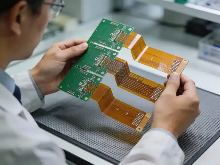
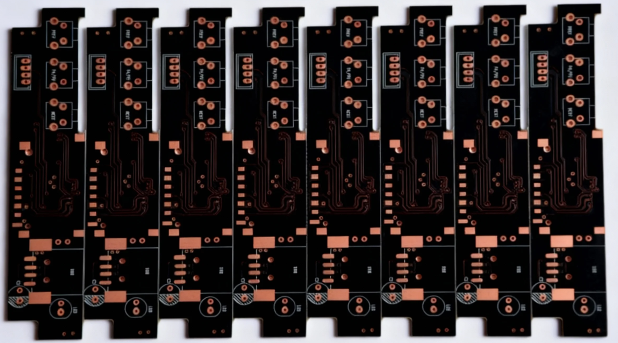
Before delving into the specifics of calculators and software, it's essential to grasp the core concepts of PCB panelization. This process involves consolidating multiple distinct PCB designs—or several copies of the same design—onto a single large panel for fabrication. This consolidated approach markedly reduces handling time, simplifies subsequent assembly stages, and ultimately lowers overall PCB cost by enabling the simultaneous production of many boards.
Critical Design Considerations
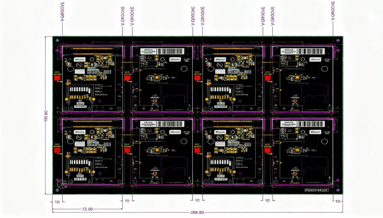
However, panelization extends beyond merely placing boards arbitrarily. Various factors must be meticulously considered, including the dimensions and geometry of individual boards, the necessary spacing for cutting (typically 2 to 3 mm between boards), and adequate clearance from the panel edges (often around 10 mm). A skillfully panelized design ensures that individual boards can be cleanly separated post-production without sustaining damage, all while optimizing the quantity of boards produced per panel.
How Can You Manually Calculate PCB Panel Size?
Manual calculation serves as a foundational exercise for comprehending the panelization process, though it can be time-intensive for more intricate designs. Here is a sequential approach to begin:
● Ascertain Board Dimensions: Begin by accurately measuring the length and width of your individual PCB design. For instance, consider a board measuring 50 mm by 30 mm.
● Factor in Spacing: Add the required spacing between boards, which is necessary for cutting or routing. A common allowance is 2.5 mm on each side. Consequently, your effective board size, inclusive of spacing, becomes 55 mm by 35 mm.
● Identify Panel Dimensions: Standard panel sizes can vary among manufacturers; however, typical dimensions are 18 inches by 24 inches (approximately 457 mm by 610 mm). Always confirm the precise panel sizes with your chosen production facility.
● Determine Fit per Axis: Divide the usable panel dimensions by your effective board size to ascertain how many boards can be accommodated along each axis. For a 457 mm x 610 mm panel, you could fit approximately 8 boards along the width (457 / 55 = 8.3, rounded down to 8) and 17 along the length (610 / 35 = 17.4, rounded down to 17). This calculation yields a total of 136 boards per panel (8 x 17).
● Incorporate Edge Clearance: It’s vital to subtract the necessary edge clearance (e.g., 10 mm on each side) from the panel's overall dimensions prior to calculating the fit. With this clearance, the effective usable area might shrink to 437 mm x 590 mm, which would reduce the fit to 7 boards along the width and 16 along the length, totaling 112 boards.
While manual computations suffice for straightforward layouts, they generally do not account for irregular board shapes, the benefits of board rotation for improved fit, or other complex manufacturing constraints. This is precisely where advanced PCB panel calculators and specialized software become indispensable.
The Impact of PCB Panel Calculators on Manufacturing Optimization
A PCB panel calculator automates the intricate process of determining the maximum number of boards that can be efficiently placed on a panel. This automation significantly reduces the time commitment and potential for human error. These tools frequently allow users to input board dimensions, desired spacing, and specific panel sizes, generating immediate layout suggestions. Certain calculators even offer a visual representation of the panel, clearly illustrating the proposed arrangement of boards.
Consider a scenario where you are working with a board measuring 75 mm by 50 mm, intended for a 400 mm by 500 mm panel. A calculator can swiftly indicate that rotating the boards by 90 degrees might increase the yield from 20 boards to 24 per panel. This type of immediate insight is invaluable for minimizing material waste and substantially enhancing manufacturing efficiency. Numerous online tools are available at no cost and are straightforward to operate, making them readily accessible even for independent designers or hobbyists. By inputting a few key numerical values, one can readily experiment with diverse layouts to identify the most economically advantageous solution.
Leveraging Advanced PCB Panelization Software for Superior Yield
While fundamental calculators are effective for simpler undertakings, sophisticated PCB panelization software elevates optimization to an entirely new echelon. These advanced programs are engineered for professional engineers and manufacturers who regularly manage intricate designs, diverse board types, or PCB mass production requirements.
Key Features of Professional Software
● Automated Nesting: The software intelligently arranges boards in the most space-efficient manner possible, frequently rotating or mirroring them to accommodate more units on a single panel. This capability can boost yield by 10-15% compared to manual layout methods.
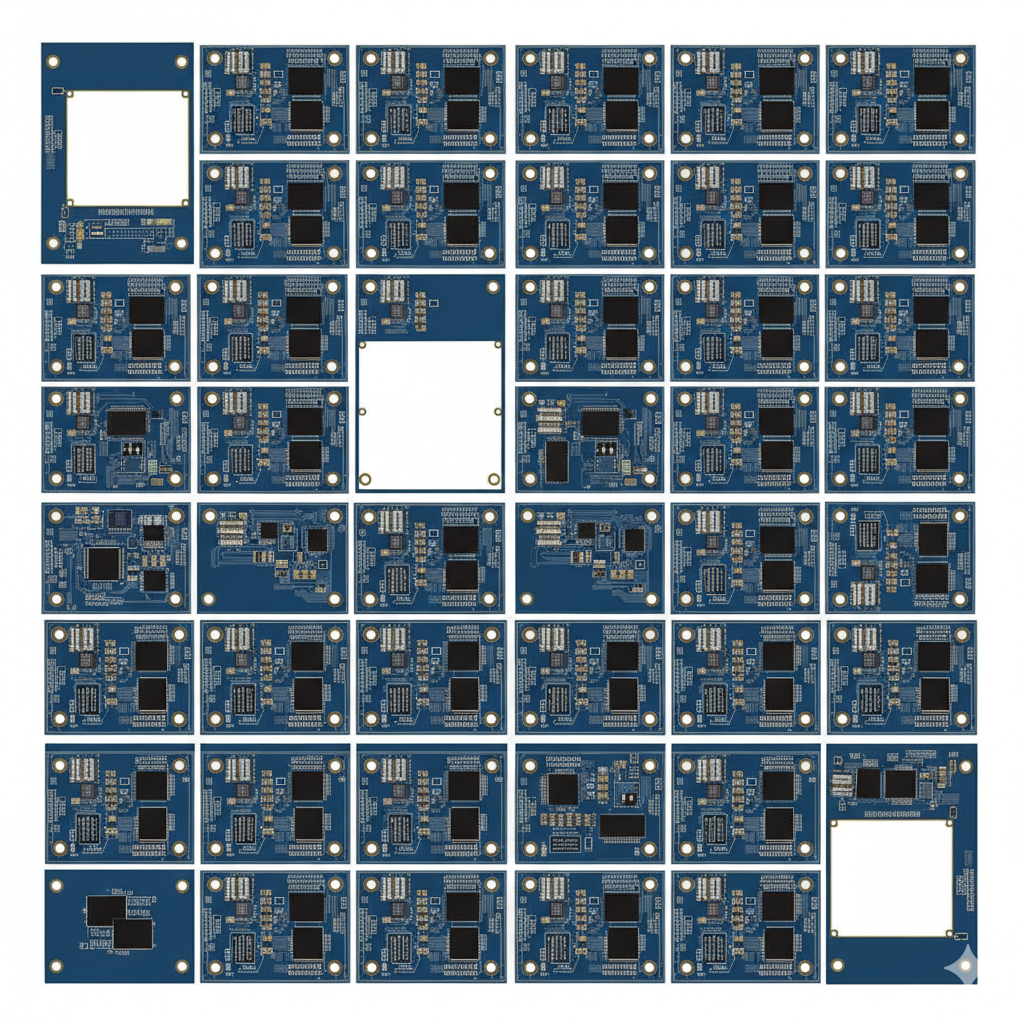
● Support for Multiple Designs: For production scenarios involving different board designs on the same panel, the software can expertly combine them to minimize any unutilized space.
● Constraint Adherence: It meticulously factors in manufacturing guidelines such as minimum spacing, edge clearance, and specific tooling requirements, thereby guaranteeing the panel is fully production-ready.
● Cost Projection: Certain tools can estimate material consumption and provide cost projections based on the proposed panel layout, assisting in budget-conscious decision-making.
By utilizing such specialized software, a PCB manufacturer might see panel utilization climb from 70% to 90%, leading to a substantial decrease in material waste. For a production run of 10,000 boards, even a 5% improvement in yield can translate into savings of hundreds of dollars in raw materials.
Advantages of Maximizing PCB Yield Per Panel
Optimizing the PCB yield per panel offers numerous benefits that directly influence both financial performance and operational efficiency.
Financial and Operational Benefits
● Reduced Costs: Fitting more boards onto each panel directly correlates with less material waste and a lower cost per individual unit. If a panel costs $50 to produce and accommodates 100 boards instead of 80, the per-board cost decreases from $0.63 to $0.50—a substantial 20% reduction.
● Accelerated Production: Producing a greater quantity of boards in a single production run diminishes the total number of panels required, thereby accelerating the manufacturing timeline. This efficiency is particularly crucial for large-volume orders where time-to-market is a critical factor.
H3: Environmental and Quality Benefits
● Environmental Stewardship: Minimizing waste reduces the volume of unused PCB materials (such as fiberglass and copper) that ultimately end up in landfills. Efficient panelization represents a small but meaningful contribution to more sustainable manufacturing practices.
● Enhanced Quality Control: Panelized boards are typically processed as a single unit, which helps ensure consistent quality across an entire batch. Furthermore, fewer panels necessitate less handling, thereby mitigating the risk of damage during various production stages.
Best Practices for Optimal PCB Panel Design
To fully capitalize on the capabilities of PCB panel calculators and optimization tools, integrating these best practices throughout the design and manufacturing phases is crucial.
Design Phase Best Practices
● Design with Panelization in Mind: Endeavor to maintain board dimensions as consistent as possible to simplify the panel layout process. Unless absolutely necessary, avoid excessively complex board shapes, as they can significantly reduce nesting efficiency.
● Proactive Communication with online pcb manufacturer: Different fabrication houses maintain unique panel sizes and specific spacing requirements. Share your design specifications early in the process to ensure full compatibility with their established manufacturing workflows.
● Strategic Use of Separation Methods: Employ breakaway tabs or V-grooves as methods to facilitate easier board separation after production, concurrently minimizing wasted space. Tabs generally necessitate 5-8 mm of space, while V-grooves typically require even less.
● Experiment with Orientations: In some instances, rotating a board by 90 or 180 degrees can dramatically improve the panel fit. Many optimization tools enable experimentation with various orientations to achieve the most favorable results.
● Allocate Space for Tooling Holes: Reserve adequate space for tooling holes or fiducial markers (typically 3-5 mm in diameter), which are essential for precise alignment during the assembly process. Position these elements in areas that do not impede board placement or functionality.
Addressing Common Challenges in PCB Panelization
Even with access to the most advanced tools, panelization can still present certain obstacles.
Overcoming Design and Production Hurdles
● Irregular Board Shapes: Non-rectangular boards frequently create empty spaces on a panel, leading to reduced yield. Utilize software equipped with sophisticated nesting algorithms to fit irregular shapes together like a puzzle, or consider redesigning the board for a more panel-friendly geometry if feasible.
● Overcrowding Issues: Positioning too many boards in excessively close proximity can result in cutting errors or damage during the separation process. Always strictly adhere to minimum spacing guidelines (typically 2-3 mm) to prevent such complications.
● Panel Size Constraints: If your manufacturer utilizes smaller panels than anticipated, your meticulously calculated layout might prove incompatible. It is imperative to verify panel dimensions upfront and design with sufficient flexibility to accommodate varying sizes.
Selecting the Appropriate PCB Panel Optimization Tools
With a plethora of PCB panel calculators and software solutions available, choosing the right tool ultimately depends on your specific requirements.
Factors to Consider for Tool Selection
● User-Friendliness: For novices or smaller-scale projects, prioritize straightforward online calculators equipped with intuitive interfaces.
● Feature Set: For professional applications, opt for software that offers advanced functionalities such as automatic nesting, multi-design support, and comprehensive manufacturing rule checks.
● Integration Capabilities: Some advanced tools seamlessly integrate with existing PCB design software, allowing for direct export of designs into a panel layout environment.
● Cost Implications: While many basic calculators are free, sophisticated software often requires a subscription or a one-time purchase. It is prudent to weigh the initial investment against the potential financial savings derived from optimized yields.
Concluding Thoughts: Optimizing PCB Production with Panel Calculators
Maximizing board yield and minimizing material waste are pivotal objectives for efficient PCB manufacturing. A PCB panel size calculator stands as an invaluable asset in achieving these goals. Regardless of whether you are performing manual layout calculations or employing advanced PCB panelization software, the correct approach can yield substantial benefits in terms of time savings, cost reductions, and enhanced sustainability within your production workflow. By meticulously adhering to best practices and fully utilizing PCB panel optimization tools, you can ensure that every square inch of material is effectively employed, resulting in the delivery of high-quality boards at a reduced cost. Initiate your exploration of various available tools today to identify the solution that best integrates with your operational processes. With a well-defined strategy, you are poised to experience significant improvements in your PCB yield per panel, thereby fostering a smoother and more profitable manufacturing endeavor.