Introduction
In high-speed electronics design, achieving electromagnetic compatibility (EMC) is essential for reliable performance. PCB stackup EMC plays a critical role in reducing electromagnetic interference (EMI), which can compromise signal integrity and cause compliance failures. As electrical engineers push clock speeds higher and integrate more complex circuits, unintended radiation and susceptibility become major concerns. Proper stackup design minimizes these issues by optimizing layer arrangement, providing shielding, and ensuring low-impedance return paths. This article explores best practices for PCB stackup EMC, focusing on ground planes, shielding techniques, and strategies for minimizing radiation. Electrical engineers will find structured guidance to implement these principles effectively in their designs.
Modern PCBs often operate in environments with dense electromagnetic fields, making EMC optimization non-negotiable. Poor stackup choices lead to excessive emissions or susceptibility, resulting in redesigns and delays. By prioritizing PCB stackup for EMC from the outset, engineers can achieve compliance with regulatory standards while enhancing overall board performance. Key elements include strategic placement of reference planes and controlled dielectric spacing. These practices not only reduce EMI but also improve power distribution and signal quality.
What Is PCB Stackup and Why EMC Matters
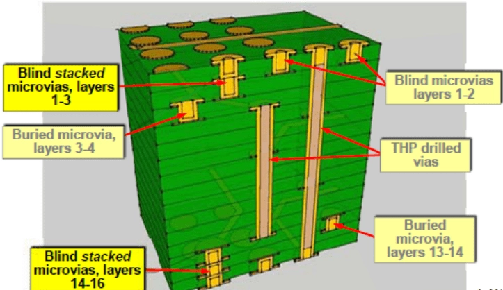
PCB stackup refers to the specific arrangement of conductive copper layers, dielectric materials, and prepregs in a multilayer board. Each layer serves a purpose, such as signal routing, power distribution, or grounding, with thicknesses and materials influencing electrical characteristics. In the context of electromagnetic compatibility, stackup determines how well the board contains internal noise and resists external interference. Effective PCB stackup EMC ensures the device functions correctly in its intended electromagnetic environment without causing or suffering undue disruption.
EMC matters because regulatory bodies mandate limits on emissions and immunity thresholds for commercial and industrial products. High-speed signals generate harmonics that radiate as EMI if not properly managed, leading to failures in tests like radiated emissions. Reducing EMI through thoughtful stackup design prevents costly iterations and supports faster time-to-market. For electrical engineers, understanding stackup impacts on impedance, crosstalk, and radiation is fundamental to robust designs. Ground planes and shielding within the stackup form the backbone of these efforts.
Failure to prioritize EMC in stackup can amplify common-mode currents on cables or enclosures, exacerbating interference. Conversely, optimized configurations provide natural shielding and low-inductance paths, aligning with industry expectations for reliability.
Technical Principles of EMI Generation in PCB Stackups
Electromagnetic interference arises primarily from time-varying currents creating magnetic fields that induce voltages in nearby conductors. In PCBs, large current loops formed by signals returning through distant paths radiate efficiently, especially at frequencies above 10 MHz. Stackup influences loop area directly; signals routed far from reference planes force returns around board edges, increasing radiation. Ground planes adjacent to signal layers confine return currents beneath traces, minimizing these loops and thus reducing EMI.
Plane resonances occur when power or ground planes act as antennas due to gaps, splits, or inadequate decoupling. These structures support standing waves at quarter-wavelength frequencies, radiating broadband noise. Proper stackup mitigates this by dedicating full layers to continuous planes and pairing power with adjacent ground for capacitance. Dielectric thickness between layers affects characteristic impedance and field containment; thinner dielectrics tighten field lines to planes, enhancing shielding.
Crosstalk between layers contributes to EMI when magnetic or electric coupling transfers noise. Stackup sequencing with ground planes between signal layers blocks this coupling orthogonally. Minimizing radiation also involves symmetry in via transitions to preserve return paths across layers.
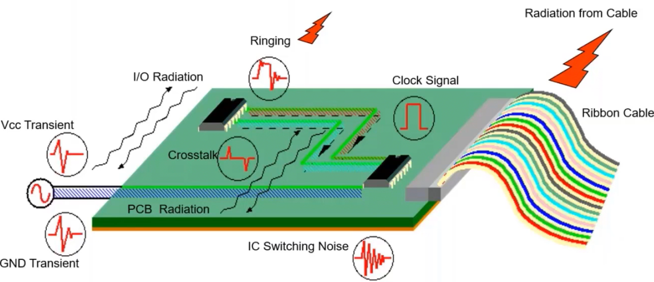
Common-mode radiation dominates far-field emissions, driven by imbalances in differential pairs or clock lines. Stackup design addresses this by providing equipotential planes that equalize potentials and suppress differential-to-common-mode conversion.
Best Practices for PCB Stackup EMC
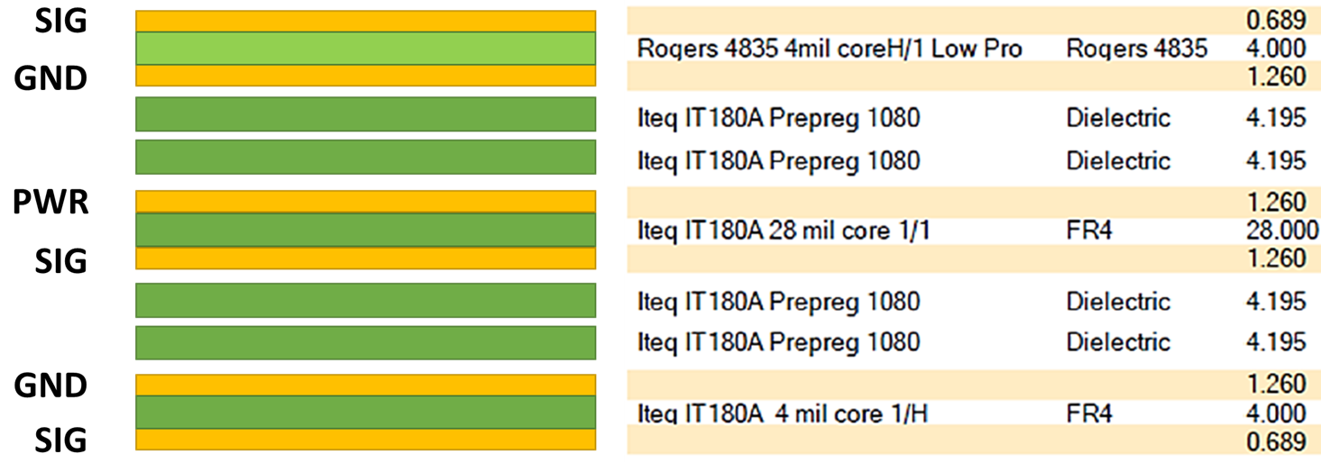
Start with the minimum layer count needed for routing density while allocating dedicated planes for ground and power. For 4-layer boards, a common EMC-optimized stackup is top signal over ground, inner power plane, and bottom signal over another ground. This configuration sandwiches signals between planes, reducing radiation by over 20 dB compared to signal-signal-power-ground arrangements. Ground planes provide shielding and low-impedance returns, critical for reducing EMI at high frequencies.
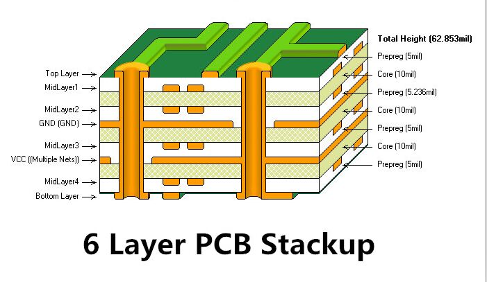
In 6-layer stackups, dedicate layers 2 and 5 to ground planes, with layer 3 for power and layers 1, 4, 6 for signals. This setup minimizes radiation by embedding sensitive signals between reference planes, forming a stripline environment. Pair power and ground closely, typically 0.1 to 0.2 mm apart using thin prepregs, to form distributed capacitance that filters noise. Avoid splitting planes under high-speed signals; IPC-2221 guidelines emphasize continuous reference planes to prevent resonances.
Shielding effectiveness improves with multiple ground planes acting as Faraday cages. Route high-speed signals on inner layers adjacent to planes rather than outer layers exposed to air. Orthogonal routing on adjacent signal layers reduces broadside coupling. For minimizing radiation, control trace lengths to below lambda/20 at the highest frequency of interest.
- 4-Layer: Signal / Ground / Power / Signal — Tight field containment, low loop areas
- 6-Layer: Signal / Ground / Power / Ground / Power / Signal — Dual shielding, balanced power distribution
- 8-Layer: Signal / Ground / Signal / Power / Power / Signal / Ground / Signal — Enhanced isolation for mixed signals
Use symmetric stackups to prevent warpage, ensuring consistent dielectric properties per IPC-6012 performance specifications. Decouple power planes with vias to ground at 1/20 wavelength intervals.
Via fencing around sensitive areas creates guard traces tied to ground, further shielding. Simulate stackup parasitics early to verify impedance matching and EMI margins.
Troubleshooting EMI Issues in PCB Stackups
Engineers often encounter emissions peaking at clock harmonics due to inadequate ground referencing. Diagnose by reviewing stackup; if signals lack adjacent planes, reroute to inner layers. Susceptibility failures indicate poor shielding; add ground pours or planes between analog and digital sections. Measure near-field emissions with probes to identify resonating planes, then stitch splits with vias.
Common pitfalls include asymmetric power-ground spacing causing inductance spikes. Remedy by thinning dielectrics between them. For mixed-signal boards, isolate planes with moats, but bridge carefully to avoid slots longer than lambda/20. IEC 61000-4-3 testing reveals radiated immunity weaknesses; optimize stackup iteratively with pre-compliance scans.
Prototype validation confirms stackup efficacy. Adjust based on sniffer probe data, focusing on return path integrity.
Conclusion
Optimizing PCB stackup for EMC demands strategic layer planning centered on ground planes, tight power-ground coupling, and shielding. These practices effectively reduce EMI, minimize radiation, and ensure electromagnetic compatibility in demanding applications. Electrical engineers benefit from structured stackups like signal-ground-power configurations, which provide low loop areas and field containment. Adhering to principles in IPC-2221 and similar standards guarantees reliable performance. Implement simulations and prototypes to refine designs, achieving compliance and superior signal integrity.
FAQs
Q1: What is the best 4-layer PCB stackup for EMC?
A1: A signal-ground-power-signal arrangement excels for PCB stackup EMC. Ground planes adjacent to signals confine return currents, reducing EMI through smaller loop areas. This setup aligns with guidelines for minimizing radiation while supporting moderate routing density. Power and ground proximity forms capacitance for noise filtering. Test pre-compliance to verify effectiveness.
Q2: How do ground planes reduce EMI in stackups?
A2: Ground planes provide low-impedance return paths, minimizing loop areas that radiate EMI. They shield signals by containing fields between layers, enhancing electromagnetic compatibility. Continuous planes prevent resonances, crucial for high-speed designs. Place them adjacent to signal layers for optimal results. Multiple planes offer additional shielding benefits.
Q3: Why pair power and ground planes closely in PCB stackup EMC?
A3: Close spacing creates distributed capacitance, decoupling noise and reducing inductance. This lowers impedance at high frequencies, aiding EMI reduction. Thin dielectrics between planes tighten coupling without excessive cost. It supports stable power delivery while minimizing radiation. Follow symmetry for mechanical stability.
Q4: What role does shielding play in minimizing radiation?
A4: Shielding via ground planes blocks crosstalk and external interference in PCB stackups. Inner signal routing between planes forms striplines with inherent shielding. This reduces susceptibility and emissions effectively. Orthogonal layouts further limit coupling. Essential for compliance in dense boards.
References
IPC-2221B — Generic Standard on Printed Board Design. IPC, 2003
IPC-6012E — Qualification and Performance Specification for Rigid Printed Boards. IPC, 2017
IEC 61000-4-3 — Electromagnetic compatibility (EMC) - Part 4-3: Testing and measurement techniques - Radiated, radio-frequency, electromagnetic field immunity test. IEC, 2020