Introduction
Printed Circuit Board (PCB) thickness plays a vital role in the design and functionality of electronic devices. For electrical engineers, understanding PCB thickness is essential to ensure structural integrity, thermal management, and electrical performance. This comprehensive guide explores the nuances of PCB thickness, including its impact on design, manufacturing, and applications like High-Density Interconnect PCBs (HDI PCBs). Additionally, it covers critical aspects such as solder mask layers and their influence on board durability and performance. Whether you are designing a compact consumer gadget or a robust industrial system, mastering PCB thickness specifications can optimize your project outcomes. Join us as we break down the technical principles, industry standards, and best practices to help you navigate this fundamental aspect of PCB engineering with precision and confidence.
What Is PCB Thickness and Why It Matters
PCB thickness refers to the total vertical dimension of a printed circuit board, typically measured in millimeters or mils. Standard thicknesses range from 0.4 mm to 3.2 mm, depending on the application and design requirements. This measurement includes the substrate material, copper layers, and additional coatings like solder mask layers. Thickness directly affects a board's mechanical strength, flexibility, and ability to dissipate heat.
For electrical engineers, PCB thickness matters because it influences signal integrity, especially in High-Density Interconnect PCBs where compact layouts demand precise control over impedance. Thicker boards provide better durability for heavy components, while thinner boards suit lightweight, portable devices. Incorrect thickness can lead to issues like warpage, poor soldering, or inadequate insulation. Hence, selecting the right thickness ensures reliability and compliance with performance expectations in diverse applications.
Technical Principles of PCB Thickness
Core Components Affecting Thickness
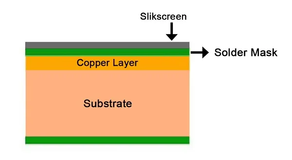
PCB thickness is determined by several layered elements. The substrate, often made of FR-4 material, forms the base and varies in thickness based on design needs. Copper layers, used for conductive traces, add to the overall dimension, with standard weights like 1 oz or 2 oz per square foot. Solder mask layers, applied as a protective coating over copper, contribute a thin but critical addition, typically around 0.01 to 0.03 mm per side. Prepreg layers, used in multilayer boards, bond the structure and further influence the final thickness.
Impact on Electrical Performance
Thickness impacts dielectric properties, affecting signal transmission in high-frequency designs. In High-Density Interconnect PCBs, thinner substrates reduce signal loss but may compromise structural stability. Engineers must balance these factors to maintain impedance control and minimize crosstalk. Standards like IPC-2221B provide guidelines for appropriate thickness selection based on voltage and current requirements.
Thermal and Mechanical Considerations
Thicker PCBs handle thermal loads better by distributing heat across a larger mass. However, excessive thickness can hinder heat dissipation in compact designs. Mechanically, thickness affects rigidity; thinner boards are prone to bending, risking trace damage. For HDI PCBs, achieving a thin profile without sacrificing strength is a common challenge, often addressed through material selection and layer optimization.
Suggested Reading: Decoding PCB Thickness: How to Optimize for Performance, Cost, and Reliability
Role of Solder Mask Layers in PCB Thickness
Solder mask layers serve as a protective barrier over copper traces, preventing oxidation and short circuits during assembly. While their contribution to overall PCB thickness is minimal, their uniform application is crucial for maintaining dimensional accuracy. Typically, solder mask thickness ranges between 0.01 mm and 0.03 mm per side, as per guidelines in IPC-SM-840E, which defines performance criteria for these coatings.
In High-Density Interconnect PCBs, solder mask application requires precision due to tight spacing between traces. Uneven layers can lead to defects like solder bridging or insufficient insulation. Engineers must specify mask thickness and type, such as liquid photoimageable or dry film, to ensure compatibility with fine-pitch components. Proper design of solder mask layers also aids in meeting environmental durability standards, enhancing the board’s lifespan in harsh conditions.
High-Density Interconnect PCBs and Thickness Challenges
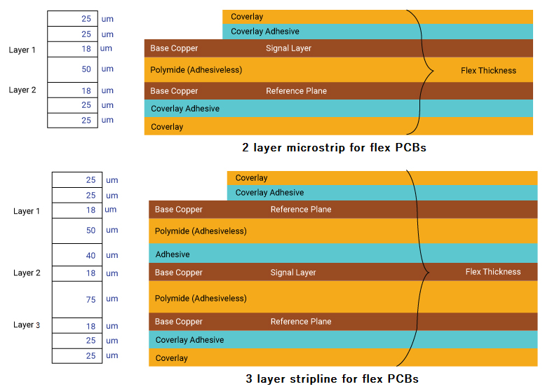
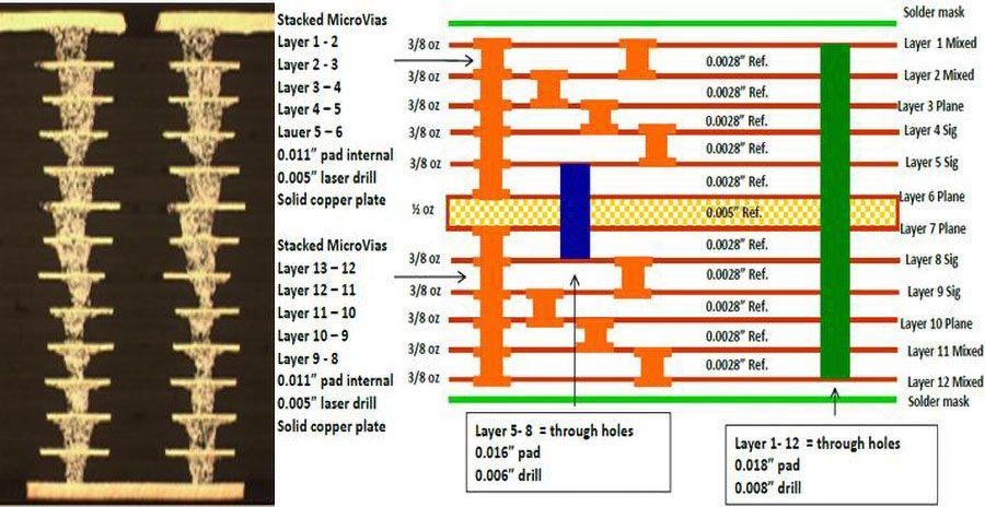
High-Density Interconnect PCBs are characterized by fine traces, microvias, and multiple layers, enabling compact designs for advanced electronics. Thickness control in HDI PCBs is critical due to the need for miniaturization without compromising performance. Standard HDI boards may range from 0.6 mm to 1.6 mm, but achieving thinner profiles often requires specialized materials and manufacturing techniques.
A primary challenge is maintaining signal integrity in thin boards. Reduced thickness can increase electromagnetic interference if not managed through proper layer stacking and grounding. Additionally, microvias used in HDI designs demand precise drilling and plating, which can be affected by substrate thickness variations. Adhering to standards like IPC-6016, which addresses HDI performance, helps engineers mitigate these risks through structured design rules.
Thermal management is another concern. Thin HDI PCBs struggle to dissipate heat from densely packed components, necessitating advanced materials with high thermal conductivity. Balancing thickness with mechanical stability ensures the board withstands assembly stresses and operational vibrations, a key consideration for portable and wearable devices.
Practical Solutions for Optimizing PCB Thickness
Material Selection
Choosing the right substrate material sets the foundation for thickness optimization. FR-4 is common for standard thicknesses due to its cost-effectiveness and reliability. For thinner HDI designs, materials with higher glass transition temperatures offer better stability. Engineers should consult IPC-4101E for material specifications to match project needs.
Layer Stackup Design
Effective layer stackup planning minimizes thickness while ensuring electrical performance. In multilayer and HDI PCBs, alternating signal and ground planes reduces noise and controls impedance. Tools adhering to IPC-2221B guidelines can simulate stackup configurations to predict outcomes before manufacturing.
Manufacturing Tolerances
Tight control over manufacturing tolerances prevents thickness deviations. Standards like IPC-6012E outline acceptable limits for board dimensions, ensuring consistency across production batches. Specifying tolerances for solder mask layers and copper thickness during design prevents cumulative errors in the final product.
Testing and Validation
Post-manufacturing testing verifies thickness compliance. Techniques like cross-sectional analysis measure layer dimensions, while mechanical tests assess warpage under stress. Following IPC-A-600K criteria for acceptability ensures the board meets visual and dimensional standards for reliability.
Best Practices for Electrical Engineers
For electrical engineers, integrating PCB thickness considerations into the design phase is essential. Begin by defining the application requirements, such as whether the board will support high-power components or fit into a compact enclosure. Use simulation software to model thermal and electrical behavior under varying thicknesses, referencing standards like IPC-2221B for conductor spacing and clearance.
When working on High-Density Interconnect PCBs, prioritize microvia reliability by adhering to aspect ratio limits specified in IPC-6016. Collaborate with manufacturing teams to confirm achievable tolerances, especially for solder mask layers, to avoid assembly issues. Always specify thickness requirements in design documentation to align with production capabilities.
Regularly review industry updates on materials and processes to stay informed about advancements in thin-board technologies. Incorporate environmental testing to validate performance under temperature and humidity extremes, ensuring compliance with standards like IPC-TM-650 for test methods. These practices collectively enhance design accuracy and product longevity.
Conclusion
PCB thickness is a fundamental parameter that shapes the performance, reliability, and manufacturability of electronic systems. From influencing signal integrity in High-Density Interconnect PCBs to ensuring proper application of solder mask layers, thickness considerations permeate every stage of design and production. Electrical engineers must navigate the interplay of material choices, layer configurations, and industry standards to achieve optimal outcomes. By adhering to established guidelines like those from IPC, professionals can address challenges and implement solutions that meet the demands of modern electronics. Understanding and controlling PCB thickness ultimately leads to robust, efficient, and innovative designs tailored to specific applications.
FAQs
Q1: How does PCB thickness affect High-Density Interconnect PCBs performance?
A1: In High-Density Interconnect PCBs, thickness significantly impacts signal integrity and thermal management. Thinner boards reduce signal loss but may increase interference if not designed properly. Standards like IPC-6016 provide guidelines for layer stacking and microvia reliability to balance compactness with performance. Engineers must prioritize precise thickness control to ensure functionality in compact, high-performance devices without risking mechanical instability.
Q2: What role do solder mask layers play in PCB durability?
A2: Solder mask layers protect copper traces from oxidation and prevent short circuits during soldering. As per IPC-SM-840E, these thin coatings enhance environmental resistance, extending PCB lifespan. Proper thickness and application ensure insulation in dense layouts, reducing risks of defects. This protection is vital for maintaining durability under harsh operating conditions, especially in industrial or outdoor applications.
Q3: Why is thickness tolerance critical in PCB manufacturing?
A3: Thickness tolerance ensures consistency across PCB production, affecting fitment and performance. Deviations can lead to assembly issues or signal problems, particularly in High-Density Interconnect PCBs. Standards like IPC-6012E define acceptable limits to maintain dimensional accuracy. Engineers must specify tolerances during design to align with manufacturing capabilities, ensuring reliable outcomes in final products.
Q4: How can engineers optimize PCB thickness for specific applications?
A4: Engineers can optimize PCB thickness by selecting appropriate materials and defining layer stackups based on application needs. Referencing IPC-2221B for design rules helps balance electrical and mechanical requirements. Testing and simulation validate choices, especially for High-Density Interconnect PCBs. Collaboration with manufacturers ensures achievable specifications, tailoring thickness to suit power, size, or environmental demands effectively.
References
IPC-2221B — Generic Standard on Printed Board Design. IPC, 2012.
IPC-6012E — Qualification and Performance Specification for Rigid Printed Boards. IPC, 2020.
IPC-6016 — Qualification and Performance Specification for High Density Interconnect (HDI) Structures. IPC, 1999.
IPC-SM-840E — Qualification and Performance of Permanent Solder Mask and Flexible Cover Materials. IPC, 2010.
IPC-A-600K — Acceptability of Printed Boards. IPC, 2020.
IPC-4101E — Specification for Base Materials for Rigid and Multilayer Printed Boards. IPC, 2017.
IPC-TM-650 — Test Methods Manual. IPC, Current Revision.