Introduction
Effective power distribution in printed circuit board (PCB) design is critical for ensuring signal integrity and minimizing noise in electronic systems. A well planned power plane and capacitor placement strategy plays a vital role in achieving stable voltage levels and reducing unwanted effects like jitter. For electrical engineers, understanding how placement depends on impedances, setting placement priority, and optimizing power planes within the stackup are key to successful designs. This article explores the technical principles behind power delivery networks (PDN), the importance of decoupling capacitors, and best practices to maintain low impedance and control jitter. By focusing on proven methods and industry standards, this guide aims to equip engineers with actionable insights for high performance PCB layouts.
What Are Power Planes and Why Do They Matter
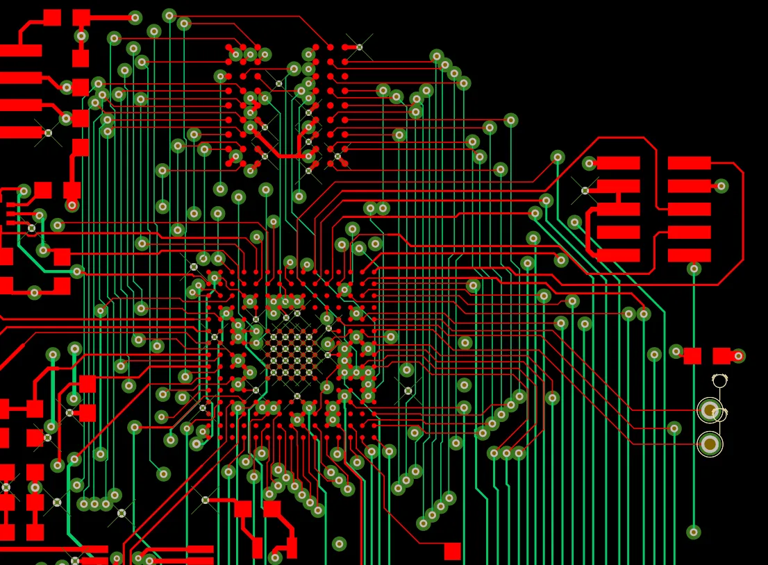
Power planes are dedicated copper layers in a PCB stackup used to distribute voltage across components. Unlike individual traces, power planes provide a low impedance path for current, ensuring stable power delivery to integrated circuits (ICs) and other active devices. Their importance lies in reducing voltage drops and minimizing electromagnetic interference (EMI), which can degrade circuit performance. For electrical engineers, power planes within a multilayer PCB are essential for high speed designs where signal integrity is paramount. Poorly designed power planes can lead to increased jitter, a timing deviation that affects clock signals and data transmission. By maintaining consistent voltage levels, power planes help mitigate such issues, making them a cornerstone of reliable PCB design.
Technical Principles of Power Planes and Capacitor Placement
Understanding Impedances in Power Delivery Networks
Impedance in a PDN refers to the opposition to current flow at various frequencies. A low impedance path is crucial for delivering clean power to ICs, especially at high frequencies where transient currents are common. High impedances can cause voltage fluctuations, leading to noise and signal degradation. Engineers must design power planes to minimize inductance, as it directly impacts impedance. The placement of power planes within the stackup affects this parameter, with closer proximity to ground planes reducing loop inductance. Standards like IPC-2221B provide guidelines for layer stackup and impedance control to ensure optimal power distribution.
Related Reading: Impedance Control with Power Plane, design
Role of Decoupling Capacitors in Noise Reduction
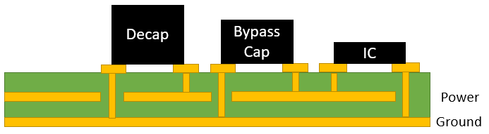
Decoupling capacitors act as local energy reservoirs, supplying transient current to ICs during switching events. They help maintain stable voltage by filtering out high frequency noise and reducing impedance at specific frequencies. Effective decoupling requires careful selection of capacitor values and their strategic placement near power pins of active components. The goal is to minimize the loop area between the capacitor, IC, and ground plane, thus lowering inductance. Without proper decoupling, voltage spikes can introduce jitter in clock signals, disrupting system timing. Following guidelines from standards like IPC-7351B ensures correct capacitor mounting and connection for optimal performance.
Placement Priority and Its Impact on Performance
Placement priority determines the order in which power planes and capacitors are positioned in the PCB layout. Prioritizing power planes closer to high speed components reduces the distance current must travel, lowering inductance and impedance. Capacitors should be placed as close as possible to IC power pins to minimize parasitic effects. Placement depends on the specific requirements of the design, including frequency range and current demand. For instance, high frequency circuits may require multiple small value capacitors near sensitive components to address rapid transients. Incorrect placement priority can result in higher jitter and reduced system reliability, especially in high speed digital designs.
Jitter and Its Relation to Power Integrity
Jitter represents timing variations in periodic signals, often caused by noise in the power supply. In high speed systems, even small voltage fluctuations can lead to significant timing errors, affecting data integrity. Power integrity directly influences jitter, as unstable voltage levels disrupt the consistent operation of oscillators and clocks. A robust PDN with low impedance power planes and effective decoupling capacitors minimizes these fluctuations. Engineers must consider jitter specifications when designing power distribution, ensuring that placement strategies align with the system's timing requirements. Adhering to standards like IPC-6012E for PCB performance helps in achieving the necessary stability.
Best Practices for Power Plane and Capacitor Placement
Optimizing Power Planes Within the Stackup
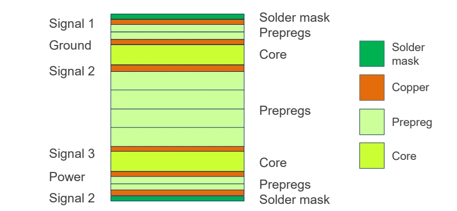
Positioning power planes within the PCB stackup requires careful planning. Place power planes adjacent to ground planes to form a natural capacitance, reducing high frequency noise. This configuration also shortens return paths for current, lowering inductance. For multilayer boards, allocate inner layers for power distribution to shield them from external interference. Ensure uniform copper distribution to avoid hot spots and maintain consistent voltage levels. Following guidelines from IPC-2221B for layer spacing and dielectric thickness aids in achieving balanced impedance across the board.
Strategic Decoupling Capacitor Placement
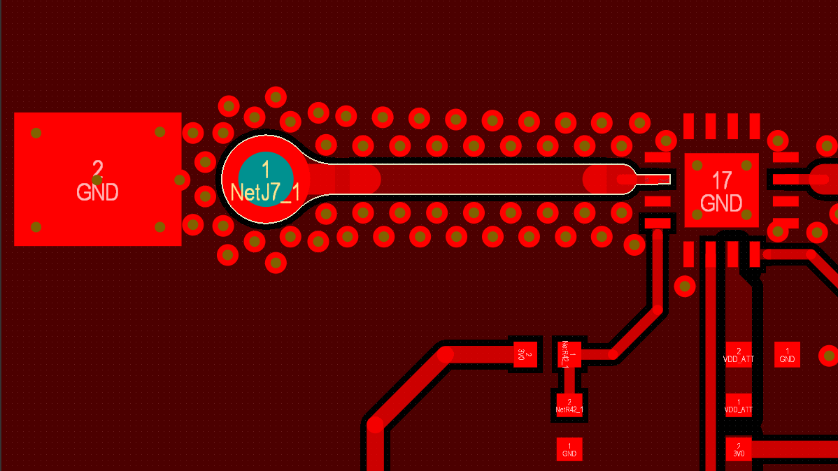
Place decoupling capacitors as close as possible to the power pins of ICs to minimize loop inductance. Use multiple capacitors with different values to cover a broad frequency range, addressing both low and high frequency noise. For example, combine small ceramic capacitors for high frequency transients with larger ones for bulk energy storage. Connect capacitors directly to power and ground planes using short, wide traces or vias to reduce resistance. Placement depends on the IC’s power requirements and should prioritize high current demand areas. Standards like IPC-7351B offer detailed recommendations for land patterns and connections.
Managing Impedances for Stable Power Delivery
To maintain low impedances, ensure power planes are continuous with minimal cuts or splits, as discontinuities increase inductance. Use via stitching to connect power and ground planes, enhancing current carrying capacity. Simulate the PDN during design to identify potential impedance peaks and adjust capacitor placement accordingly. Tools adhering to industry standards can predict impedance behavior at different frequencies, guiding engineers in optimizing layouts. Regular spacing of decoupling capacitors across the board helps in maintaining a uniform impedance profile, reducing the risk of voltage drops.
Mitigating Jitter Through Design Techniques
Reducing jitter starts with a stable power supply. Minimize noise by using dedicated power planes for sensitive analog and digital sections, preventing crosstalk. Implement proper grounding techniques, such as a solid ground plane, to provide a clean return path. Place high frequency decoupling capacitors near clock circuits to filter out noise affecting timing. Regularly review timing budgets and jitter specifications during design to ensure compliance with system requirements. Following IPC-6012E standards for board qualification ensures that manufacturing processes do not introduce additional noise sources.
Related Reading: Power Plane Decoupling: A Comprehensive Guide to PCB Stability
Troubleshooting Common Issues in Power Distribution
Power distribution issues often manifest as excessive noise or unexpected jitter in high speed systems. If voltage fluctuations are observed, verify the placement of decoupling capacitors and ensure they are connected with minimal loop area. Check for splits in power planes that might increase impedance and disrupt current flow. Use simulation tools to analyze the PDN for resonance frequencies that could amplify noise. If jitter exceeds acceptable limits, inspect the proximity of power planes within the stackup to critical components. Adjusting capacitor values or adding additional ones near problematic areas can often resolve these issues. Always refer to standards like IPC-A-600K for acceptability criteria during inspection and testing.
Conclusion
A strategic approach to power plane and capacitor placement is essential for achieving reliable power distribution in PCB designs. By focusing on low impedances, correct placement priority, and optimal positioning of power planes within the stackup, engineers can significantly enhance system performance. Effective decoupling strategies further reduce noise, ensuring stable voltage levels and minimizing jitter in high speed applications. Adhering to established industry standards provides a solid foundation for addressing power integrity challenges. With careful planning and attention to detail, electrical engineers can design PCBs that meet the stringent demands of modern electronic systems.
FAQs
Q1: How does placement priority affect power plane performance?
A1: Placement priority directly impacts power plane performance by determining how close power layers are to critical components. Positioning power planes near high speed ICs reduces inductance and ensures stable voltage delivery. Following industry standards for stackup design helps in prioritizing layers effectively, minimizing noise and enhancing signal integrity for optimal system operation.
Q2: What role do impedances play in PCB power distribution?
A2: Impedances in a power delivery network influence how effectively current is supplied to components. High impedances can cause voltage drops and noise, disrupting circuit operation. Designing power planes and capacitor networks to maintain low impedance across frequencies is crucial for stable power delivery and reducing issues like signal degradation.
Q3: Why is decoupling important for reducing jitter?
A3: Decoupling capacitors are vital for reducing jitter by providing local current during switching events, stabilizing voltage levels. They filter high frequency noise that can disrupt timing signals. Proper placement near IC power pins ensures minimal inductance, maintaining clean power and preventing timing variations in high speed designs.
Q4: How should power planes within a stackup be arranged?
A4: Power planes within a PCB stackup should be placed adjacent to ground planes to form natural capacitance and reduce noise. Inner layers are ideal for power distribution to shield from interference. This arrangement lowers loop inductance and supports stable voltage, adhering to guidelines for multilayer board design.
References
IPC-2221B — Generic Standard on Printed Board Design. IPC, 2012.
IPC-7351B — Generic Requirements for Surface Mount Design and Land Pattern Standard. IPC, 2010.
IPC-6012E — Qualification and Performance Specification for Rigid Printed Boards. IPC, 2020.
IPC-A-600K — Acceptability of Printed Boards. IPC, 2020.