What Is Power Plane Decoupling and Why Is It Crucial for PCBs?
Power plane decoupling is a fundamental technique in Printed Circuit Board (PCB) design, meticulously employed to stabilize the voltage supply delivered to integrated circuits (ICs) and other electronic components. Its primary objective is to mitigate unwanted noise and voltage fluctuations within the power delivery network. When ICs rapidly change their operational states, they draw sudden, brief surges of current. These abrupt demands can induce transient voltage drops or spikes in the power supply, phenomena collectively known as power supply noise. Such disturbances can severely degrade signal integrity, generate electromagnetic interference (EMI), and, in extreme cases, lead to complete system failures.
The core principle of decoupling involves strategically placing capacitors in close proximity to ICs, where they act as localized energy reservoirs. These capacitors efficiently supply the instantaneous current demands of the ICs, thereby buffering the impact of noise and ensuring a consistently stable voltage—an essential design practice across all types of PCB board, from consumer electronics to high-performance computing systems. Without adequate decoupling, a circuit risks experiencing issues such as ground bounce—a condition where the ground plane's voltage fluctuates due to rapid current changes—which can disrupt normal circuit operation. This guide will delve into the critical role of decoupling capacitors, explore best practices for their placement, and outline proven strategies to reduce ground bounce and general power supply noise, empowering designers to create more robust and efficient circuits.
Understanding the Function of Power Plane Decoupling Capacitors
Power plane decoupling capacitors, often referred to as bypass capacitors, are indispensable components in modern PCB design. Their main purpose is twofold: to filter out high-frequency noise from the power supply and to provide a stable, instantaneous voltage source to ICs during periods of rapid current demand. These capacitors serve as a vital buffer, storing electrical charge locally and releasing it swiftly when an IC requires a sudden surge of current.
Types of Decoupling Capacitors
Typically, two main categories of decoupling capacitors are utilized in PCB designs:
● Bulk Capacitors: These are generally larger capacitance devices (ranging from 10 μF to 100 μF). Their role is to address lower-frequency noise components and serve as a substantial charge reservoir for the entire board, smoothing out larger voltage variations.
● Ceramic Capacitors: Characterized by smaller capacitance values (commonly 0.01 μF to 1 μF), these capacitors are specifically designed to handle high-frequency noise. Their efficacy is maximized when placed as close as possible to the ICs, allowing for immediate current delivery to suppress high-speed transients.
The overall effectiveness of a decoupling strategy is highly dependent on the capacitor's value, its inherent type, and its precise physical placement. For instance, a 0.1 μF ceramic capacitor is frequently chosen for its ability to suppress high-frequency noise directly at an IC's power pin, while a larger 10 μF tantalum capacitor might be positioned further afield to manage lower-frequency fluctuations across the power plane. Without the judicious application of these capacitors, the impedance of the Power Delivery Network (PDN) can become unacceptably high at certain critical frequencies, leading to pronounced voltage drops. A meticulously engineered decoupling strategy aims to maintain the PDN impedance below a specified target—often less than 1 mΩ at critical operational frequencies—thereby safeguarding signal integrity.
Optimal Capacitor Placement for Peak Performance
The strategic positioning of decoupling capacitors is as vital as their selection. Suboptimal placement can negate the intended benefits of decoupling, leaving the circuit susceptible to noise and ground bounce. Adhering to specific guidelines for capacitor placement is crucial for achieving an effective PCB layout.
Key Placement Guidelines
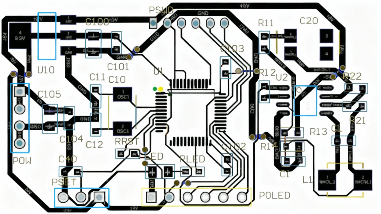
1. Proximity to IC Power Pins: The closer a decoupling capacitor is located to an IC's power pin, the more effective it becomes. This minimizes the parasitic inductance of the connecting traces, enabling faster and more efficient current delivery. Ideally, capacitors should be positioned within 1-2 mm of the power pin. For high-speed ICs, such as microcontrollers or FPGAs, this proximity is even more critical for maintaining stable operation.
2. Short, Wide Connections: Long and narrow traces introduce undesirable inductance, which can impede a capacitor's ability to respond rapidly to sudden current demands. Instead, utilize short, wide traces or connect the capacitor directly to the power and ground planes through dedicated vias. This approach significantly reduces loop inductance, ideally keeping it below 1 nH for demanding high-frequency applications.
3. Multi-Capacitor Strategy for Frequency Coverage: A single capacitor value cannot effectively attenuate noise across the entire spectrum of problematic frequencies. Employ a combination of capacitors with varying values (e.g., 0.01 μF, 0.1 μF, and 1 μF) adjacent to each IC. This layered approach ensures comprehensive noise suppression across a broad frequency range. The capacitor with the smallest value, targeting the highest frequencies, should be placed closest to the power pin, followed by larger values for mid-range frequency filtering.
4. Distributed Bulk Capacitance: For larger PCBs populated with numerous ICs, distributing bulk capacitors strategically across the power plane is essential. This ensures that a stable voltage is maintained uniformly throughout the entire board, effectively preventing voltage drops in areas distant from the main power supply input.
Effective Strategies for Ground Bounce Reduction
Ground bounce is a prevalent issue in high-speed digital circuits, characterized by fluctuations in the ground plane voltage caused by the rapid, simultaneous switching of IC outputs. This phenomenon can lead to erroneous signal triggering and degraded circuit performance. Mitigating ground bounce requires a combination of robust decoupling and thoughtful PCB design practices.
Proven Ground Bounce Mitigation Techniques
1. Minimize Loop Inductance: Ground bounce primarily arises from inductance within the power and ground return paths. By meticulously placing decoupling capacitors extremely close to IC power pins and utilizing low-inductance connections (such as very short, wide traces or direct vias to planes), the voltage fluctuations on the ground plane can be significantly reduced. For high-speed designs, targeting a loop inductance of less than 0.5 nH is often recommended.
2. Continuous Ground Planes: A solid, unbroken ground plane is paramount for providing a low-impedance return path for all currents. This continuity is crucial for reducing the likelihood and severity of ground bounce. Avoid partitioning the ground plane unless absolutely necessary, as splits can create high-impedance paths that exacerbate noise issues.
3. Limit Simultaneous Switching Outputs (SSO): Ground bounce intensifies when multiple outputs of an IC switch states at precisely the same moment. Where feasible, design the circuit to stagger switching events or select ICs equipped with built-in slew rate control, which moderates the rate of current change, thereby reducing the transient impact.
4. Local Ground Vias: For ICs that feature multiple ground pins, it is best practice to connect each individual ground pin directly to the solid ground plane with its own dedicated via. This minimizes the inductance of each ground connection and ensures return currents are distributed more evenly, effectively reducing localized ground bounce.
Advanced Power Supply Noise Reduction Techniques
Beyond the fundamental principles of proper decoupling capacitor placement, several advanced strategies can be employed to further diminish power supply noise in your PCB designs, thereby improving the performance of sensitive analog and digital circuits.
Supplementary Noise Reduction Methods
1. Optimized Power Plane Design: Design power planes to exhibit low impedance across an extensive range of frequencies. Utilize wide power traces or dedicate entire planes to minimize both resistance and inductance. For multilayer boards, positioning power and ground planes adjacently creates a natural interplane capacitance (typically around 1 nF per square inch), which is highly effective in suppressing high-frequency noise.
2. Ferrite Beads for Enhanced Filtering: Ferrite beads, when placed in series with the power supply line, act as a frequency-dependent resistor, effectively filtering out high-frequency noise before it can propagate to sensitive components. Combining a ferrite bead with a bulk capacitor creates a powerful low-pass filter, significantly reducing noise above 1 MHz.
3. Isolation of Sensitive Circuits: In mixed-signal designs, it is crucial to electrically isolate analog and digital sections of the board. This prevents high-frequency digital switching noise from coupling into and corrupting sensitive analog circuits. This can be achieved through separate power planes or by using split planes that connect at a single, well-defined point, thereby maintaining a clean reference ground for analog components.
4. PDN Impedance Monitoring: Employ sophisticated simulation tools to analyze the impedance profile of your power delivery network across various frequencies. The goal is to maintain an impedance below 1 mΩ at the critical operating frequencies of your ICs, ensuring minimal voltage ripple. Adjust capacitor values and their placements based on these simulation results to achieve optimal performance.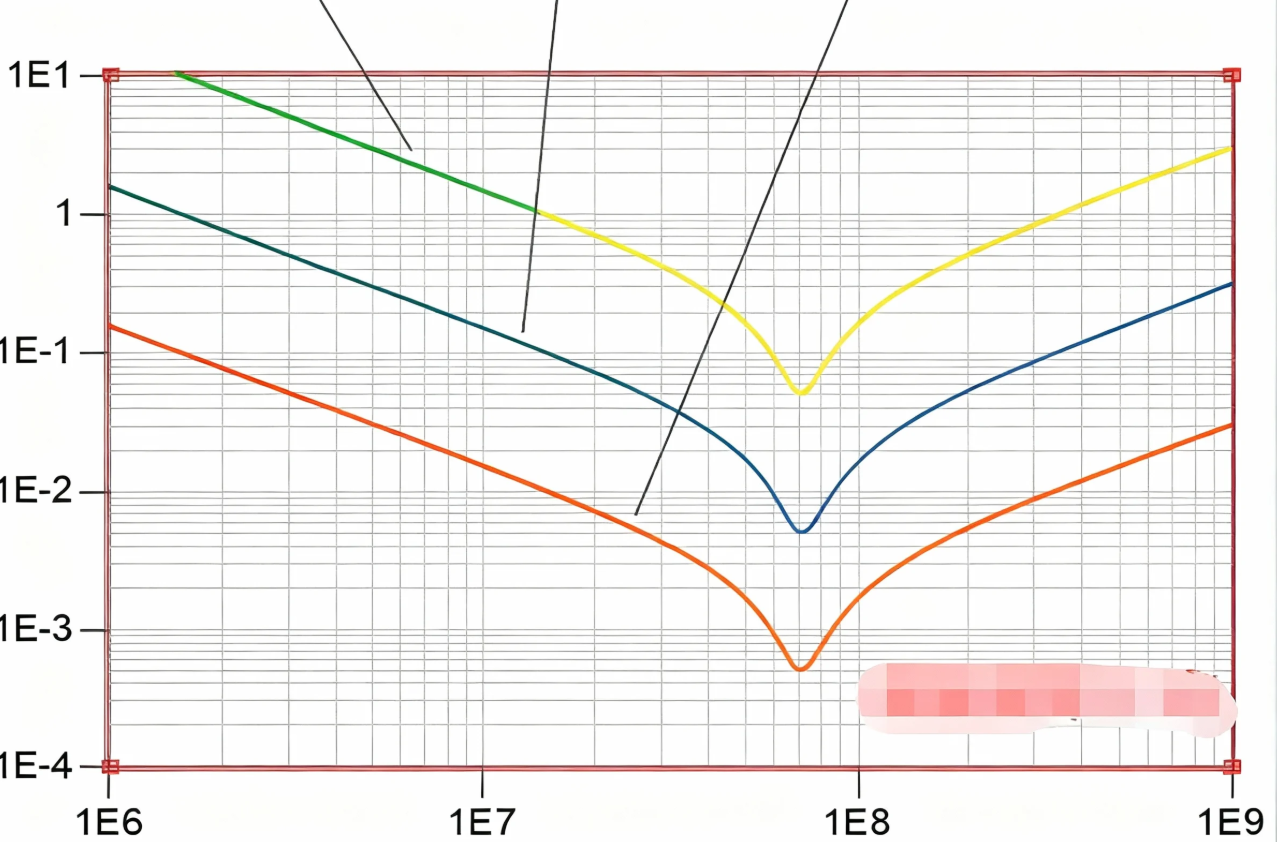
Comprehensive Decoupling Strategies for PCB Design
Having covered the fundamentals of power plane decoupling capacitors, their placement, and noise reduction techniques, let's synthesize this knowledge into actionable, comprehensive decoupling strategies for your PCB designs. These strategies are designed to ensure reliable power delivery and robust signal integrity, even in complex and high-speed applications.
Integrated Decoupling Approaches
1. Layer Stackup Optimization: Meticulously plan your PCB layer stackup to inherently minimize noise. Position power and ground planes on adjacent layers to maximize the interplane capacitance; this natural capacitance is highly effective for high-frequency decoupling. For instance, in a 4-layer board, a common and effective stackup might be Signal-Power-Ground-Signal, ensuring tight electromagnetic coupling between the power and ground planes.
2. Diverse Capacitor Value Spectrum: As previously discussed, a single capacitor value cannot adequately address noise across the entire frequency range. Implement a combination of capacitor values—such as 0.01 μF, 0.1 μF, and 10 μF—to effectively cover a broad frequency spectrum, typically from 100 kHz up to 100 MHz. This multi-value approach ensures comprehensive noise suppression across the operational bandwidth of your circuit.
3. Simulation and Rigorous Testing: Before finalizing your PCB layout, it is imperative to simulate the power delivery network (PDN) to identify any potential issues with impedance, resonance, or voltage ripple. Utilizing tools like SPICE or specialized PDN analysis software can help you precisely fine-tune capacitor values and their exact placement. Post-fabrication, meticulously test your physical board with an oscilloscope to measure voltage ripple and confirm that noise levels are well within acceptable limits (e.g., typically less than 50 mV peak-to-peak for most digital ICs).
4. Adherence to Manufacturer Guidelines: Many IC manufacturers provide specific decoupling recommendations within their component datasheets. These valuable guidelines often include suggested capacitor values, critical placement distances, and even illustrative layout diagrams. Always consult and adhere to these documents to ensure compliance with the IC's precise requirements for stable and optimal operation.
Common Decoupling Mistakes to Avoid
Even seasoned designers can inadvertently make errors in power plane decoupling that can undermine a PCB's performance. Being aware of these common pitfalls can prevent significant issues in your design.
Frequent Decoupling Errors
● Excessive Distance from ICs: A prevalent mistake is placing decoupling capacitors too far from their target ICs. Increased distance introduces additional parasitic inductance in the connection, which severely diminishes the capacitor's ability to supply instantaneous current and thus reduces its overall effectiveness. Proximity should always take precedence in layout decisions.
● Insufficient Capacitor Coverage: Relying on a single capacitor or an inadequate range of capacitor values is another common error. This approach fails to provide comprehensive noise suppression across the wide spectrum of frequencies that can cause problems. A multi-capacitor strategy is essential for broad protection.
● Compromising Ground Plane Integrity: Introducing cuts, splits, or isolated islands within the ground plane is a critical mistake. Such disruptions create high-impedance return paths for current, exacerbating ground bounce, increasing EMI, and degrading overall signal integrity. A solid, continuous ground plane is non-negotiable for reliable performance.
● Neglecting PDN Simulation: Skipping the Power Delivery Network (PDN) simulation phase can lead to unforeseen resonance points or impedance mismatches within the power system. These issues often only become apparent after the PCB has been fabricated, leading to costly and time-consuming redesigns. Always simulate to predict and mitigate problems beforehand.
Conclusion: Mastering Power Plane Decoupling for Superior PCB Performance
Effective power plane decoupling is a cornerstone of reliable and high-performance PCB design. By thoroughly understanding the critical role of decoupling capacitors, mastering optimal capacitor placement strategies, and diligently implementing techniques for reducing ground bounce and power supply noise, designers can dramatically enhance the stability and overall performance of their electronic circuits. These principles are universally applicable, whether you are developing a straightforward microcontroller project or a complex, high-speed system.
Begin by selecting the appropriate combination of capacitor types and values for your specific design needs. Ensure these capacitors are placed strategically in close proximity to IC power pins. Always prioritize the use of a continuous and robust ground plane to minimize noise and provide stable reference points. Leverage advanced simulation tools to fine-tune your power delivery network, meticulously verify its impedance characteristics, and always adhere to the specific recommendations provided by component manufacturers for the most optimal results. With these comprehensive decoupling strategies, you are well-equipped to confidently tackle even the most demanding PCB designs and achieve exceptional circuit performance.


