Introduction
Electronics prototyping allows hobbyists to turn ideas into working circuits quickly and affordably. PCB prototyping with embedded components takes this to the next level by integrating resistors, capacitors, and other passives directly into the board layers. This approach shrinks designs, improves signal integrity, and reduces parasitic effects compared to traditional surface-mount methods. For electronic hobbyists experimenting with compact devices like wearables or IoT sensors, understanding embedded components opens doors to advanced electronics prototyping. PCB fabrication and assembly processes become more intricate, but the rewards include higher reliability and smaller footprints. This guide walks beginners through the essentials, from concepts to practical steps.
What Are Embedded Component PCBs and Why Do They Matter?
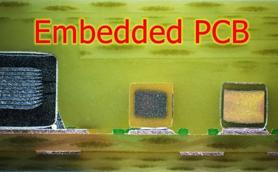
Embedded component PCBs place passive elements inside the laminate structure rather than on the surface. These components connect via vias or traces built into the layers during PCB fabrication. Hobbyists benefit from denser boards that fit into tight spaces, ideal for portable projects. In electronics prototyping, embedded designs cut assembly time since fewer surface parts need placement. They also enhance performance by shortening signal paths and minimizing inductance. As projects grow complex, mastering PCB prototyping with embedded components becomes key for reliable outcomes.
The relevance stems from modern demands for miniaturization. Traditional PCBs stack components externally, leading to larger boards and potential interference. Embedded versions integrate seamlessly, supporting high-frequency signals better. For beginners, starting with simple embedded passives builds confidence before tackling full systems. PCB assembly focuses only on active devices and remaining passives, streamlining the workflow. Overall, this technique matters for hobbyists pushing boundaries in custom electronics.
Key Technical Principles of Embedded Components
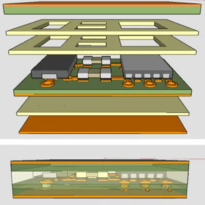
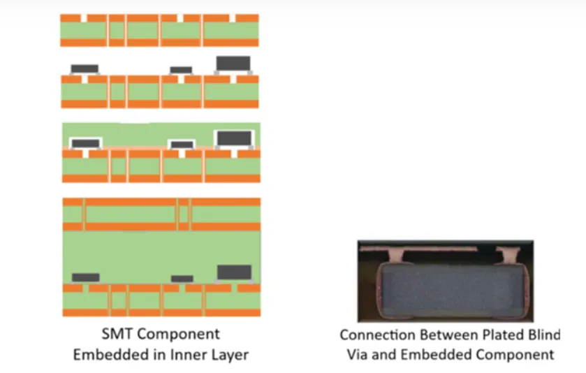
Embedded components rely on precise layer buildup during PCB fabrication. Manufacturers create cavities in core layers using mechanical routing or laser ablation, then insert components before lamination. Vias or plated through-holes provide electrical connections, ensuring continuity across layers. Adhesives or direct bonding secure parts, while resin encapsulation protects them from environmental stress. According to IPC-7092, design rules emphasize component positioning near signal layers to optimize integrity. Thermal expansion matching between materials prevents delamination over time.
Passive embedding dominates for beginners, with capacitors and resistors most common. Thin-film or polymer thick-film technologies form resistors directly on inner layers. Capacitors use ceramic dies in cavities or laminated dielectrics. Fabrication tolerances demand tight control to avoid misalignment during pressing. Signal integrity improves as embedded parts reduce loop areas for electromagnetic interference. Hobbyists should grasp these principles to avoid common pitfalls in prototyping.
Active components like ICs pose higher challenges due to heat and pin density. They require advanced cooling vias and precise registration. Standards guide material selection for reliability. Layer stackup planning integrates embeds without disrupting routing. Electrical testing verifies functionality post-fabrication. These mechanisms form the foundation for successful PCB prototyping.
The Step-by-Step PCB Prototyping Process for Embedded Components
Start with schematic capture, selecting embeddable passives from datasheets. Layout software must support cavity definitions and net assignments for buried parts. Generate Gerber files, drill files, and stackup drawings specifying embedded locations. Include notes on component types and tolerances for the fabricator. This design phase sets the stage for accurate PCB fabrication.
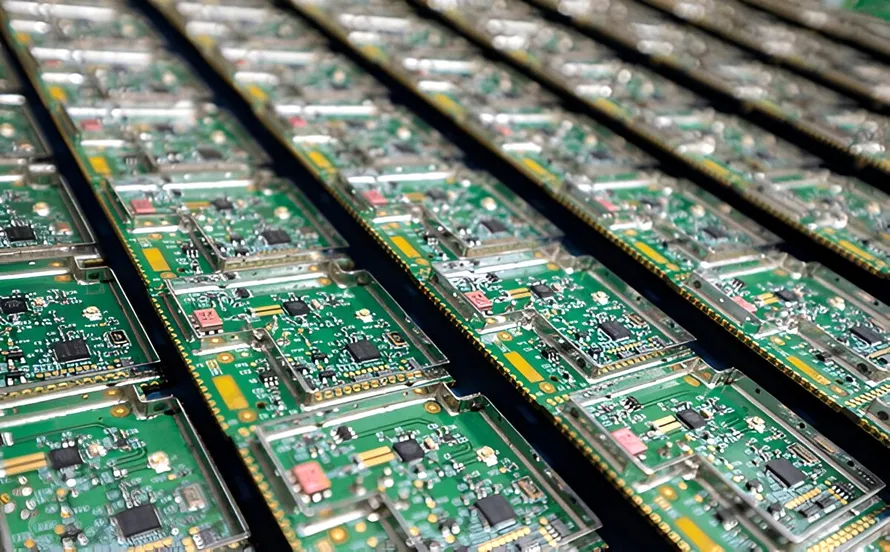
In PCB fabrication, the panel undergoes sequential buildup. Cores receive cavities, components get placed via pick-and-place or manual for prototypes. Laminators apply pressure and heat to encapsulate, followed by via drilling and plating. Outer layers pattern with imaging and etching. Electrical test probes check continuity, including embedded nets. Finishes like ENIG apply for solderability.
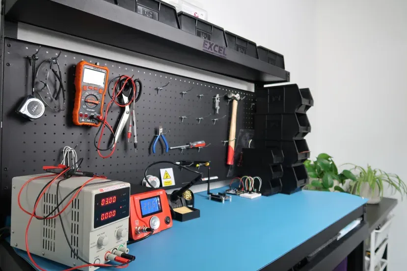
PCB assembly handles surface-mount elements post-fabrication. Stencils aid solder paste application for remaining passives and actives. Reflow soldering follows J-STD-001 guidelines for joint quality. Inspection confirms no bridges or voids. Functional testing validates the full circuit. Hobbyists iterate by ordering small batches.
Best Practices for PCB Prototyping with Embedded Components
Choose fabricators experienced in embedded processes to ensure precision. Specify stackup clearly, with layer thicknesses accommodating component heights. Use fiducials for alignment during placement and lamination. Simulate thermal profiles to predict stress on embeds. Keep via sizes standard to aid plating uniformity. These steps minimize defects in electronics prototyping.
Design for testability by routing test points to embedded nets where possible. Limit embed count in first prototypes to learn the process. Select components with wide tolerances for hobbyist runs. Verify impedance control if high-speed signals involved. Document deviations from standard flows for future orders. Practical adherence boosts success rates.
In PCB assembly, clean surfaces thoroughly before reflow to avoid contamination affecting buried parts. Bake boards to remove moisture per JEDEC guidelines. Use X-ray inspection for hidden joints if available. Profile ovens match component ratings. These practices align with industry norms for reliable prototypes.
Common Challenges and Troubleshooting in Embedded PCB Prototyping
Alignment shifts during lamination challenge prototypes, causing opens. Troubleshoot by tightening fab specs on pressure and temperature. Review stackup for CTE mismatches leading to cracks. X-ray confirms placement post-build. Iterative redesign refines tolerances.
Thermal management issues arise as embeds trap heat. Add thermal vias near high-power passives. Monitor junction temperatures in testing. Adjust copper pours for spreading. Proactive design prevents failures.
Cost and lead times exceed standard PCBs due to complexity. Start small, prototype subsets first. Communicate needs clearly to fabricators. Balance embed benefits against overhead. Troubleshooting focuses on root causes like process variation.
Assembly defects like tombstoning affect surface parts interacting with embeds. Optimize reflow profiles per J-STD-001. Inspect solder joints visually and electrically. Replace faulty boards quickly in small runs. Patience yields robust results.
Conclusion
Prototyping embedded component PCBs empowers electronic hobbyists with compact, high-performance designs. Grasping principles, processes, and practices ensures smooth PCB fabrication and assembly. Standards like IPC-7092 guide reliable implementation. Start simple, iterate thoughtfully, and scale complexity. This approach transforms ideas into functional prototypes efficiently.
FAQs
Q1: What is PCB prototyping with embedded components?
A1: PCB prototyping involves creating test boards with passives buried in layers during fabrication. This electronics prototyping method reduces size and improves signals. Beginners design layouts specifying cavities, order from capable services, then assemble surfaces. Follow IPC-7092 for process guidelines. Results offer denser circuits for hobby projects.
Q2: How does PCB fabrication differ for embedded components?
A2: Fabrication adds cavity formation and component insertion before lamination. Precise alignment and encapsulation protect embeds. Stackups account for heights to avoid shorts. Testing verifies buried connections. Hobbyists gain reliability but face longer times. Standards ensure quality.
Q3: What are best practices for PCB assembly in embedded prototypes?
A3: Clean and bake boards pre-reflow per J-STD-001. Use stencils for paste, inspect joints. Test functionality fully. Limit surface density near embeds. Troubleshoot with multimeters and scopes. This yields working prototypes reliably.
Q4: Common mistakes to avoid in electronics prototyping with embeds?
A4: Overlooking CTE mismatch causes cracks. Poor cavity specs lead to misalignment. Skipping simulations risks signals. Start with few embeds, verify fab capabilities. Iterate based on tests. Avoids costly respins.
References
IPC-7092 — Design and Assembly Process Implementation for Embedded Components. IPC, 2015
IPC J-STD-001J — Requirements for Soldered Electrical and Electronic Assemblies. IPC, 2024
IPC-A-610J — Acceptability of Electronic Assemblies. IPC, 2024