Introduction
High-layer-count printed circuit boards, typically those with eight or more layers, enable complex routing for high-speed signals and dense component integration in modern electronics. However, these designs amplify electromagnetic interference (EMI) risks due to closely spaced traces, fast edge rates, and multiple signal layers. PCB EMI shielding and PCB grounding techniques become essential to maintain signal integrity, ensure regulatory compliance, and prevent system failures. Effective implementation minimizes radiated and conducted emissions while reducing susceptibility to external noise. This article explores structured approaches to shielding and grounding tailored for high-layer count PCB design, drawing on established engineering principles. Engineers can apply these methods to optimize performance in demanding applications like telecommunications and computing systems.
Understanding EMI in High-Layer-Count PCBs
Electromagnetic interference refers to unwanted noise that disrupts signal quality through coupling mechanisms in PCB layouts. In high-layer-count boards, EMI arises from sources such as clock generators, power converters, and data buses operating at gigahertz frequencies. Radiated EMI propagates through the air as electromagnetic waves, while conducted EMI travels along power lines or interconnects. Dense routing increases crosstalk between adjacent layers, exacerbating these issues. Poor management leads to bit errors, reduced margins in eye diagrams, and failure in electromagnetic compatibility tests. Addressing EMI early in the design phase preserves functionality and avoids costly redesigns.
High-layer count PCB design demands careful consideration of layer interactions, where thin dielectrics between planes can form unintended capacitors or inductors. Clock harmonics and switching transients create broad-spectrum emissions that couple capacitively or inductively. Compliance with industry emission limits requires proactive mitigation rather than post-fabrication fixes. Grounding inconsistencies further amplify EMI by creating high-impedance return paths. Engineers must prioritize low-inductance structures to contain fields within the board boundaries.
Principles of EMI Generation and Propagation
EMI generation stems from time-varying currents producing magnetic fields and voltage gradients inducing electric fields, per fundamental Maxwell's equations. Current loops act as antennas, with loop area and frequency determining radiation efficiency. In multilayer boards, signals referenced to distant grounds form large loops, radiating more effectively. Capacitive coupling occurs between parallel traces on adjacent layers, while inductive coupling links overlapping current paths. Minimizing these mechanisms involves shortening return paths and isolating sensitive areas.
Propagation within the PCB occurs via plane resonances, where cavities between power and ground planes support standing waves at specific frequencies. High-layer counts introduce multiple such cavities, each potentially radiating if excited. Edge effects launch emissions from board peripheries, especially without shielding. Understanding these principles guides the placement of ground planes as return paths and barriers. IPC-2221 outlines design parameters to control trace spacing and plane continuity, reducing coupling risks.
PCB EMI Shielding Techniques
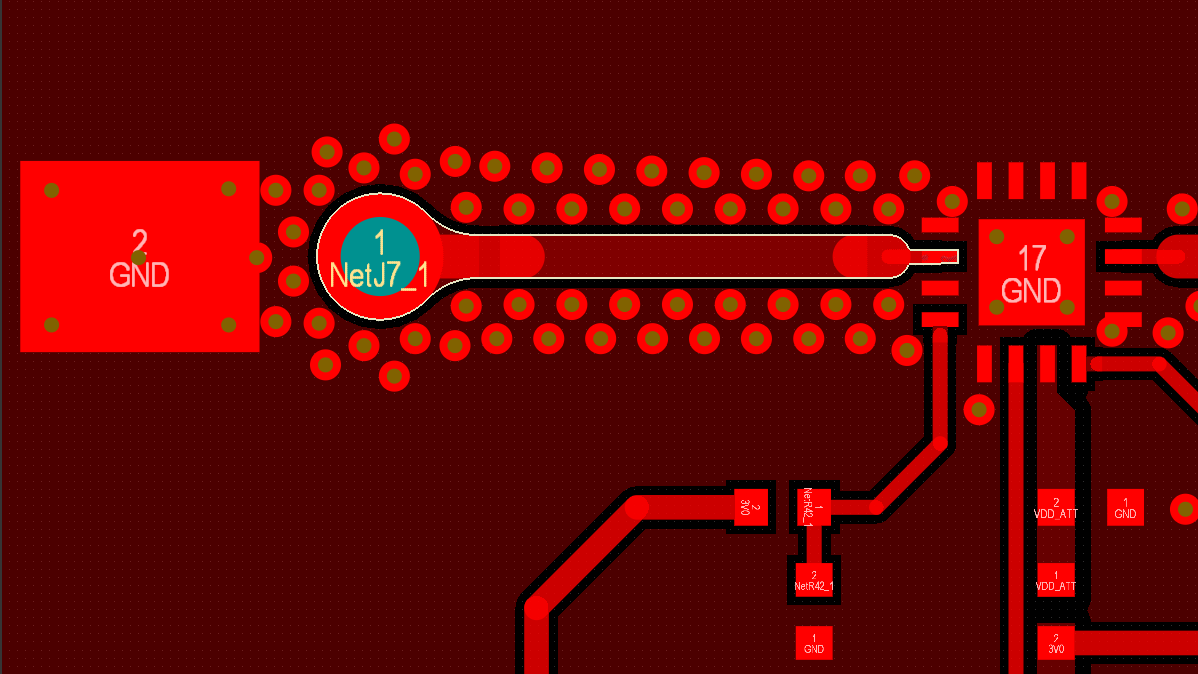
Ground planes serve as primary shields by providing low-impedance barriers that reflect and absorb electromagnetic fields. Positioning a dedicated ground plane adjacent to signal layers confines fields between them, attenuating crosstalk by over 20 dB in typical configurations. Full copper pours on inner layers block far-field radiation from outer traces. For high-frequency signals, multiple ground planes interleave with signal layers to shorten field loops. Vias connecting these planes form fences that further isolate sections.
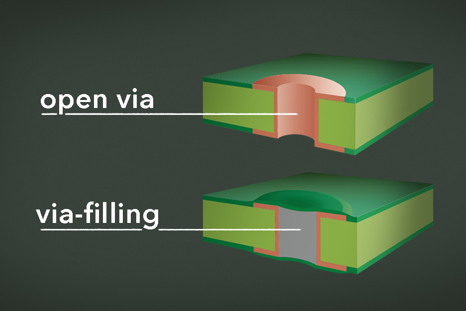
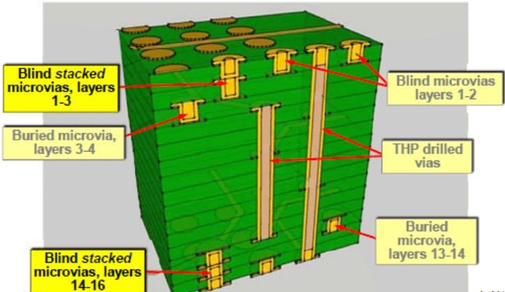
Via shielding involves arrays of grounded vias along sensitive trace edges, creating a Faraday cage-like barrier. Stitch vias every quarter-wavelength along ground-plane edges to suppress slot antennas formed by gaps. Guard traces, flanked by grounded vias, protect high-speed lines from adjacent noise. These techniques prove effective in high-layer count PCB design, where layer transitions demand robust containment. Combining planes and vias reduces emissions without altering routing density.
Related Reading: Reducing EMI in PCB Prototyping: Shielding Techniques and Grounding Strategies
Shielding enclosures, such as metal cans over noisy components, integrate with board-level planes for comprehensive protection. Connect enclosures to ground at multiple points to avoid resonances. In multilayer boards, embedded shielding layers using conductive foils add attenuation for extreme cases. Select materials with high conductivity and low permeability for broad-spectrum coverage. These methods complement grounding to achieve balanced EMI control.
PCB Grounding Techniques for High-Layer-Count Designs
Solid ground planes offer the lowest impedance paths for return currents, distributing noise evenly and preventing hot spots. Dedicate entire layers to ground in high-layer counts, avoiding splits unless partitioning analog and digital sections. Connect all ground vias to these planes with minimal stubs to maintain continuity. Multiple ground planes reduce inductance between signal layers, improving shielding effectiveness. IPC-6012E specifies performance criteria for plane integrity in rigid boards, ensuring reliability under thermal stress.
Partitioning grounds requires careful stitching to prevent slots that radiate EMI. Use dense via fields at partition boundaries to bridge planes, maintaining low-impedance paths. Separate noisy digital grounds from precision analog ones, joining them at a single point near the power entry. This hybrid approach minimizes common-impedance coupling in complex designs. Monitor plane potential with simulation to verify uniformity.
Related Reading: Improve Your Designs with the Best PCB Grounding Techniques
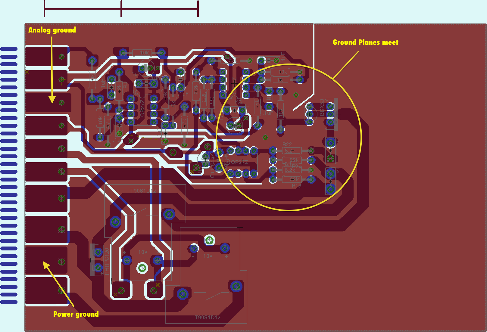
Star grounding suits low-frequency applications but yields to plane strategies in high-speed boards due to inductance. Implement hybrid grounding by routing low-current returns as stars on planes. Place decoupling capacitors strategically between power and ground planes, with vias directly to each. These techniques enhance stability in high-layer count PCB design.
Best Practices in High-Layer Count PCB Design for EMI Reduction
Optimize stackups by alternating signal and plane layers, starting with ground on layers 2 and 3 for outer signal protection. Control dielectric thicknesses to balance impedance and coupling. Route high-speed signals between planes, avoiding outer layers for clocks. Minimize trace lengths and bends to reduce loop areas. Group related signals with dedicated reference planes.
Incorporate filtering at sources: ferrites on inputs and bypass networks near ICs. Ensure plane voids are covered with stitching vias. Review impedance profiles across frequencies. These practices align with PCB grounding techniques and shielding for holistic EMI management.
Fabrication tolerances impact shielding; maintain plane etch uniformity per standards. Test prototypes with near-field probes to validate designs.
Common Challenges and Troubleshooting
Ground bounce plagues high-layer boards when simultaneous switching overwhelms planes. Mitigate with additional decoupling and wider planes. Slot resonances from splits require via fences. Crosstalk in dense routing demands microstrip over stripline transitions. Systematic reviews catch these early.
Conclusion
Reducing EMI in high-layer-count PCBs hinges on integrated PCB EMI shielding and PCB grounding techniques, from solid planes to via arrays. These methods control emissions, enhance integrity, and ensure compliance. Engineers benefit from structured stackups and partitioning for optimal results. Implementing these principles yields reliable, high-performance boards.
FAQs
Q1: What are effective PCB EMI shielding techniques for high-layer count PCB design?
A1: PCB EMI shielding techniques include dedicated ground planes adjacent to signal layers, via fences along edges, and guard traces with stitching. These create barriers that reflect and absorb fields, reducing radiated emissions. In high-layer counts, interleaving planes minimizes cavity resonances. Follow consistent plane pours to avoid slots. This approach maintains signal quality without sacrificing density.
Q2: How do PCB grounding techniques reduce EMI in multilayer boards?
A2: PCB grounding techniques use full ground planes for low-impedance returns, stitching vias for continuity, and partitioning with bridges. Multiple planes distribute currents evenly, suppressing bounce and coupling. Connect components directly to planes via short paths. Avoid splits except for isolation, joining at power inputs. These ensure stable references in high-layer count PCB design.
Q3: Why are ground planes critical in high-layer count PCB design for EMI control?
A3: Ground planes act as shields and return paths, confining fields and minimizing loop areas. In high-layer counts, they prevent interlayer crosstalk and edge radiation. IPC-2221 recommends continuous pours for effective shielding. Multiple planes lower inductance for high speeds. Proper implementation complies with performance specs like IPC-6012E.
Q4: What common mistakes undermine PCB EMI shielding efforts?
A4: Common mistakes include ground plane splits without stitching, distant return paths, and outer-layer high-speed routing. These create antennas and resonances. Neglecting via density allows leakage. Always verify stackups for plane adjacency. Correcting early avoids redesigns in high-layer count PCB design.
References
IPC-2221B — Generic Standard on Printed Board Design. IPC, 2012
IPC-6012E — Qualification and Performance Specification for Rigid Printed Boards. IPC, 2017