Introduction
In the fast-paced world of electronics manufacturing, efficient PCB assembly is crucial for meeting tight deadlines and minimizing errors. Rigid PCB silkscreen plays a pivotal role by providing clear visual cues that guide technicians during component placement and soldering. This layer includes essential rigid PCB component designators and rigid PCB markings, which streamline the entire assembly process from prototyping to high-volume production. Without proper silkscreen implementation, even the most meticulously designed rigid PCBs can lead to costly rework and delays. Engineers must prioritize rigid PCB silkscreen design rules to ensure readability and durability under real-world conditions. This article explores the fundamentals, best practices, and technical considerations for optimizing silkscreen on rigid PCBs.
What Is Rigid PCB Silkscreen and Why It Matters
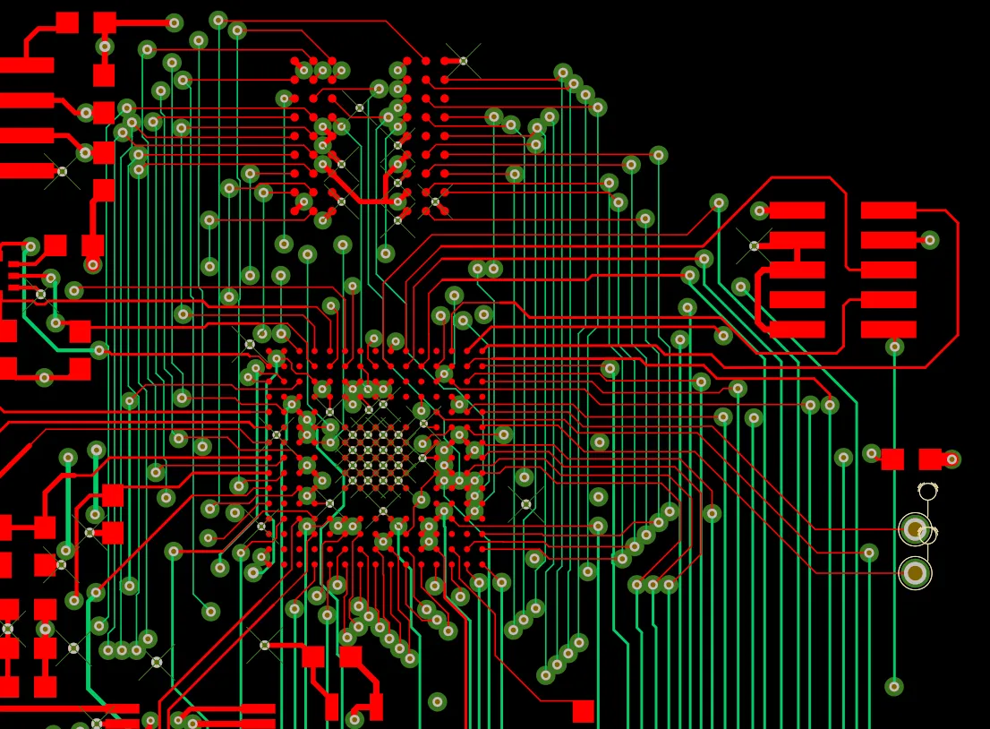
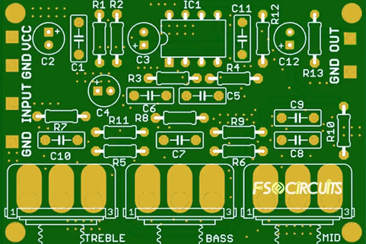
Rigid PCB silkscreen refers to the printed legend layer applied over the solder mask on rigid printed circuit boards. It consists of non-conductive inks that form text, symbols, and lines to identify components and provide assembly instructions. Common elements include rigid PCB component designators such as R1 for resistors or U5 for integrated circuits, along with rigid PCB markings like polarity indicators and pin-one identifiers. This layer is typically screen-printed using stencils and cured to withstand soldering temperatures and environmental stresses.
The importance of rigid PCB silkscreen cannot be overstated in assembly workflows. Clear markings reduce the time technicians spend cross-referencing schematics, lowering the risk of misplacement errors that could compromise board functionality. In high-mix production environments, where multiple board variants are assembled daily, precise silkscreen aids quick identification and verification. Moreover, it supports post-assembly troubleshooting by enabling field repairs without extensive documentation. Adhering to rigid PCB silkscreen design rules ensures compliance with quality expectations across the supply chain.
Technical Principles of Rigid PCB Silkscreen
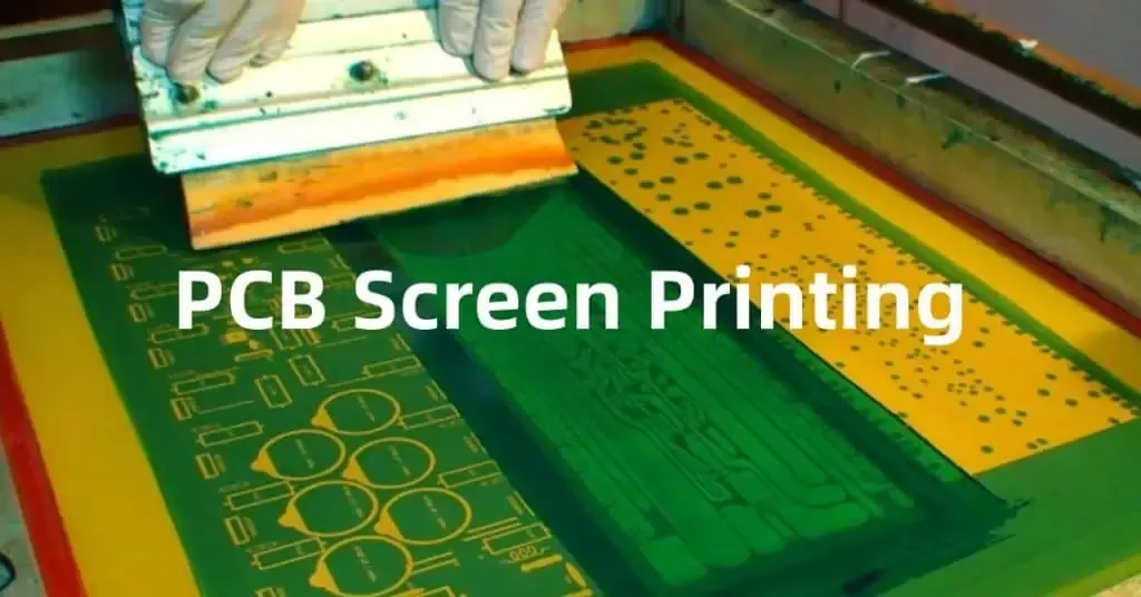
The foundation of rigid PCB silkscreen lies in the ink formulation and application process. Inks are typically epoxy-based or UV-curable polymers formulated for adhesion to the solder mask surface while resisting abrasion and chemicals. Screen printing remains the dominant method, where a mesh stencil transfers ink onto the board in precise patterns. The ink is then dried or cured using thermal ovens or UV lamps to achieve permanence.
Key engineering considerations include contrast and legibility, which depend on ink color selection against the solder mask background. White or yellow inks on green masks provide optimal visibility, while matte finishes minimize glare during inspection. The silkscreen must endure multiple reflow cycles without cracking or peeling, maintaining integrity through thermal expansion mismatches between layers. Rigid PCB markings, such as beveled triangles for pin one, follow standardized shapes to prevent orientation mistakes. These principles ensure the silkscreen serves as a reliable interface between design intent and manufacturing execution.
Material durability is governed by performance specifications that test adhesion, solder heat resistance, and solvent resistance. Engineers evaluate silkscreen quality through visual and tactile inspections post-fabrication. Variations in ink viscosity during printing can affect line definition, necessitating controlled process parameters like squeegee pressure and speed.
Rigid PCB Component Designators: Standards and Implementation
Rigid PCB component designators are alphanumeric labels uniquely identifying each component on the board. They follow a hierarchical scheme, such as starting with reference prefixes (R for resistors, C for capacitors) followed by sequential numbers. Consistent placement adjacent to the component footprint enhances usability, allowing assemblers to match physical parts to the bill of materials effortlessly.
Designators must balance density with readability, avoiding overlap with pads or traces. In multi-layer rigid PCBs, top-side designators suffice for surface-mount parts, while through-hole components may require bottom-side duplicates. Polarity markings complement designators by indicating directionality for diodes, LEDs, and electrolytic capacitors using bars, arrows, or triangles. These rigid PCB markings prevent reverse insertion, which could lead to immediate failures during power-up.
IPC-A-600 provides acceptability criteria for legend legibility, specifying minimum stroke widths and character proportions for different quality classes. Compliance ensures designators remain discernible under magnification typical in assembly lines.
Rigid PCB Markings: Beyond Designators for Assembly Guidance
Rigid PCB markings extend functionality by including fiducial marks, board outlines, and test point labels. Fiducials are small circular or cross-shaped features aiding automated optical inspection and pick-and-place alignment. Assembly-specific markings, like no-population zones or orientation guides, prevent errors in mixed-technology boards combining SMT and through-hole.
Markings must maintain spacing from solder joints to avoid flux entrapment or contamination during reflow. Engineers position them outside the keep-out zones defined by component footprints. Durable inks ensure markings survive wave soldering or selective soldering processes without fading.
Strategic use of rigid PCB markings accelerates quality control, as inspectors can verify populations at a glance. In rigid flex transitions, if applicable, markings clarify hybrid assembly sequences.
Rigid PCB Silkscreen Design Rules: Essential Guidelines
Rigid PCB silkscreen design rules form the backbone of reliable implementation. Minimum line widths and spacings ensure print fidelity, preventing bridging or voids during fabrication. Characters should use simple, sans-serif fonts to maximize stroke uniformity and reduce printing defects.
Clearance rules dictate at least 0.1 mm separation from exposed copper to avoid shorts from ink bleed. Orientation consistency, with all text readable from the same side, simplifies handling. Color coding, such as red for high-voltage warnings, adds interpretive layers without cluttering the layout.
IPC-6012 outlines performance requirements for rigid boards, including silkscreen adhesion after thermal stress. Designers iterate layouts using Gerber viewers to validate rules pre-production.
Best practices include scaling designators proportionally to component size, larger for fine-pitch ICs. Avoid fine details under 6 mil lines, as they risk washout in processing.
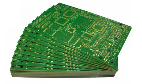
Manufacturing Process for Rigid PCB Silkscreen
Silkscreen application occurs late in the rigid PCB fabrication sequence, after solder mask curing. Panels are aligned under the screen, and ink is forced through emulsion-blocked areas. Multi-color printing requires precise registration between layers.
Post-print curing solidifies the ink, typically at 150 degrees C for epoxy types. Quality checks involve solvent rub tests and thermal shock simulations. Variations in panel warpage can distort prints, so flatness control is critical.
Best Practices for Rigid PCB Silkscreen Optimization
Start with schematic-driven automation to generate designators, ensuring synchronization with netlists. Define layer-specific rules in design software, enforcing clearances algorithmically. Prototype small batches to validate print quality under actual inks.
Collaborate with fabricators early on ink compatibility, especially for matte vs glossy masks. For high-reliability applications, opt for reinforced inks tested to IPC standards. Regular audits of silkscreen yield data refine future designs.
Incorporate version numbers and date codes in silkscreen for traceability. Limit text density to prevent overcrowding, prioritizing critical rigid PCB component designators.
Troubleshooting Common Rigid PCB Silkscreen Issues
Blurry designators often stem from ink viscosity mismatches or screen wear, resolvable by recalibrating print parameters. Fading markings post-reflow indicate insufficient cure, addressed by extending oven dwell times. Misregistration appears as offset text, fixed via improved fiducial-based alignment.
Peeling occurs from poor adhesion, mitigated by plasma cleaning pre-print. Engineers document root causes in failure modes to prevent recurrence. IPC-A-600 criteria guide acceptance decisions during incoming inspections.
Conclusion
Rigid PCB silkscreen is indispensable for transforming complex designs into assemblable realities through precise component designators and markings. Mastering rigid PCB silkscreen design rules ensures legibility, durability, and efficiency across the product lifecycle. By integrating standards-driven practices, engineers minimize assembly errors and accelerate time-to-market. Prioritizing these elements elevates overall PCB quality, supporting reliable electronics deployment.
FAQs
Q1: What are the key rigid PCB silkscreen design rules for component designators?
A1: Rigid PCB silkscreen design rules emphasize minimum clearances from pads, consistent orientation, and legible fonts. Designators should align closely with footprints without overlapping solder areas. Use sans-serif styles for uniform printing, and ensure contrast against the mask color. Standards like IPC-6012 guide adhesion and visibility requirements. Following these prevents assembly mix-ups and rework.
Q2: Why are rigid PCB markings critical for assembly processes?
A2: Rigid PCB markings such as polarity symbols and pin-one indicators prevent incorrect component orientation, reducing failures during soldering. They speed up manual and automated placement by providing visual references. Clear markings also aid inspection and repair without schematics. Durability ensures they withstand reflow and handling stresses. Proper implementation cuts production time significantly.
Q3: How does IPC-A-600 apply to rigid PCB silkscreen quality?
A3: IPC-A-600 defines acceptability for silkscreen legibility across board classes, specifying stroke width and completeness criteria. It evaluates designators and markings post-fabrication under inspection conditions. Compliance verifies readability for assembly technicians. Non-conformances like voids or smudges trigger rejects. This standard bridges design and manufacturing expectations effectively.
Q4: What factors affect rigid PCB component designators durability?
A4: Ink type, curing process, and thermal exposure influence rigid PCB component designators longevity. Epoxy inks resist abrasion better than basic types. Proper screen tension avoids defects during printing. Testing per IPC guidelines confirms performance after environmental stresses. Consistent processes yield reliable markings for long-term use.
References
IPC-A-600K — Acceptability of Printed Boards. IPC, 2020
IPC-6012E — Qualification and Performance Specification for Rigid Printed Boards. IPC, 2017