Introduction
Rigid PCB solder mask serves as a critical protective coating on printed circuit boards, safeguarding copper traces from environmental hazards and oxidation during assembly and operation. This thin polymer layer defines solderable areas, preventing unintended solder bridges and enhancing overall board reliability in demanding electronic applications. For electric engineers designing high-performance systems, understanding rigid PCB solder mask application ensures optimal solderability and long-term durability. Factory processes align this layer precisely to meet performance specifications, making it indispensable for rigid board manufacturing. As boards evolve with denser layouts, the solder mask adapts to maintain electrical integrity and mechanical strength. Proper implementation directly impacts yield rates and field performance.
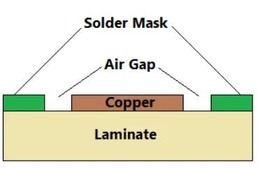
What Is Rigid PCB Solder Mask and Why It Matters
Rigid PCB solder mask is a permanent, non-conductive lacquer applied over the bare copper on a rigid printed circuit board, leaving only pads and vias exposed for soldering. Composed typically of epoxy resins or acrylics, it provides insulation against shorts, moisture ingress, and mechanical abrasion. In manufacturing, this layer matters because it controls solder flow during reflow, reducing defects like bridging or insufficient wetting. Without it, exposed traces would oxidize rapidly, compromising solder joint quality and board lifespan. Engineers rely on it for high-density interconnects where trace spacing is minimal. Compliance with standards like IPC-6012 ensures the mask integrates seamlessly with rigid board substrates for reliable operation.
The relevance extends to thermal management, as the mask influences heat dissipation from traces beneath it. Factory insights reveal that a well-applied mask minimizes warpage during soldering by balancing stresses across the board. It also facilitates automated optical inspection, aiding quality control in production lines. For electric engineers, selecting the right mask formulation prevents issues like delamination under thermal cycling. Ultimately, it bridges design intent with manufacturability, supporting applications from consumer electronics to industrial controls.
Technical Principles of Rigid PCB Solder Mask
The core mechanism of rigid PCB solder mask involves selective application and curing to form a durable barrier with precise openings over conductive features. Liquid photoimageable masks, common in modern fabs, use UV exposure through artwork to define patterns, followed by development and thermal cure for hardness. This process achieves fine resolution suitable for fine-pitch components, outperforming traditional screen printing in density. Adhesion to copper and laminate relies on surface preparation like plasma cleaning, ensuring no voids form under thermal stress. Electrical properties include high dielectric strength, preventing arcing in high-voltage designs.
Curing transforms the mask from a liquid to a cross-linked polymer, imparting resistance to solvents, chemicals, and abrasion. Factory-driven testing verifies flexibility over rigid substrates, avoiding cracks during board flexure. The mask's opacity aids in contrast for silkscreen legends, enhancing traceability. Engineers must consider its thermal coefficient matching the base laminate to mitigate CTE mismatch issues. These principles underpin why rigid PCB solder mask elevates board performance beyond basic protection.
Rigid PCB Solder Mask Application Processes
Rigid PCB solder mask application begins with surface preparation, where etched panels undergo micro-etching or oxidation to promote wetting. Screen printing applies thick-film masks for coarser features, using stencil squeegees to deposit ink evenly across the board. Photoimageable variants involve spin-coating or curtain-coating for uniform thin films, then exposing to UV light patterned by film positives. Development removes unexposed areas with aqueous solutions, revealing pads precisely. Final UV and thermal curing solidifies the layer, typically in conveyor ovens for controlled profiles.
Post-application, tack-dry and final cure steps eliminate volatiles, preventing bubbles or pinholes that could expose copper. Factory alignment tolerances ensure mask registration matches copper features within microns, critical for BGA and QFN assembly. Electroless nickel immersion gold over pads complements the mask by preventing oxidation during storage. Engineers appreciate how these steps per IPC-SM-840 qualification enhance solder joint formation. Variations like dry film lamination suit high-volume runs with consistent thickness.

Rigid PCB Solder Mask Colors
Rigid PCB solder mask colors range from the ubiquitous green to alternatives like black, blue, red, white, and matte variants, each influencing visibility and performance. Green dominates due to its balance of contrast against copper and silkscreen, facilitating inspection under standard lighting. Black masks offer superior opacity for high-contrast legends but may absorb more IR during soldering, requiring process adjustments. Blue provides excellent trace visibility for debugging, ideal for prototyping phases.
White suits LED backlighting applications where light transmission matters, though it demands careful formulation for UV cure efficacy. Yellow enhances gold pad distinction in high-reliability boards. Color choice affects manufacturability; darker pigments like black can reduce resolution in photoimaging due to light scattering. Factory insights recommend testing colors for specific wavelengths in optical AOI systems. For electric engineers, matching color to application optimizes aesthetics without compromising function.
Rigid PCB Solder Mask Design Rules
Rigid PCB solder mask design rules emphasize clearances to prevent bridging while ensuring coverage over traces. Minimum mask dams between pads typically exceed trace width to avoid solder wicking under the mask during reflow. Via tenting options cover or leave open depending on assembly needs, with rules dictating pullback from annular rings. Engineers must specify expansion or shrinkage compensation in Gerber files to account for imaging tolerances.
Overhangs on trace edges provide creepage distance for high-voltage isolation. Factory processes align rules to IPC-A-600 acceptability criteria, inspecting for voids, adhesion, and thickness uniformity. Protrusions or webbing at corners signal design flaws like insufficient clearances. Incorporating these rules early avoids costly respins. For dense layouts, photoimageable masks excel in adhering to tight rules down to fine features.
Best Practices for Rigid PCB Solder Mask Implementation
Adopt liquid photoimageable solder masks for boards under 0.15mm pitch to leverage superior resolution and thinner profiles. Verify panel cleanliness pre-application to maximize adhesion, using cross-cut tests per standards. Specify matte finishes for reduced glare in high-volume inspection. Balance cure times to achieve hardness without brittleness, monitoring via durometer readings.
Integrate mask data with drill and route in panelization for uniform processing. Post-cure plasma treatment enhances cleanliness for HASL or ENIG finishes. Engineers should simulate reflow profiles to predict mask-solder interactions. Factory audits confirm compliance through peel strength and thermal shock tests. These practices yield robust boards ready for assembly challenges.
Common defects like pinholes or delamination stem from contamination or CTE mismatch, addressable via material selection and process controls. White spots indicate incomplete cure, while orange peel texture signals poor wetting. Troubleshooting involves microscopic analysis and cross-sectioning. Proactive design reviews incorporating rules prevent recurrence.
Conclusion
Rigid PCB solder mask stands as a cornerstone of board protection and assembly success, integrating seamlessly to shield traces and guide solder precisely. From application techniques to color selections and design rules, each aspect demands factory precision aligned with engineering needs. Electric engineers benefit from its role in enhancing reliability across thermal and mechanical stresses. Mastering these elements optimizes manufacturability and performance. Prioritizing standards ensures consistent outcomes in production.
FAQs
Q1: What are the primary benefits of rigid PCB solder mask application?
A1: Rigid PCB solder mask application protects copper from oxidation, prevents solder bridges, and insulates traces for reliable operation. Factory processes like photoimaging ensure precise pad definition, improving reflow yields. It also enhances mechanical durability against handling and environmental exposure. Overall, it bridges design and assembly for high-performance boards.
Q2: Which rigid PCB solder mask colors are most suitable for electric engineers?
A2: Green rigid PCB solder mask offers optimal contrast for inspection, while blue aids trace visibility in prototyping. Black provides high opacity for legends but requires IR adjustments. White fits backlit designs. Selection depends on AOI compatibility and application needs, with factory testing recommended.
Q3: What key rigid PCB solder mask design rules should engineers follow?
A3: Rigid PCB solder mask design rules include adequate pad-to-pad clearances to avoid bridging and via pullback for annular ring exposure. Compensate for imaging shrinkage in artwork. Ensure trace overhangs for creepage. Align with acceptability criteria to facilitate manufacturing without defects.
Q4: How does rigid PCB solder mask improve solderability?
A4: Rigid PCB solder mask improves solderability by defining precise pad areas, preventing excess flow onto traces. It protects surrounding copper from oxidation pre-assembly. Compatible formulations withstand reflow temperatures without degrading. This results in clean joints and higher first-pass yields in production.
References
IPC-SM-840D — Qualification and Performance Specification for Permanent Solder Mask. IPC, 2018
IPC-6012E — Qualification and Performance Specification for Rigid Printed Boards. IPC, 2017
IPC-A-600K — Acceptability of Printed Boards. IPC, 2020


