Introduction
In modern rigid PCB designs, vias serve as critical interconnects between layers, enabling complex multilayer stackups essential for high-density electronics. As signal speeds increase into the gigahertz range, the performance of these vias directly influences overall signal integrity, with parasitic effects like inductance becoming dominant concerns. Poor via design can lead to signal reflections, overshoot, and crosstalk, compromising system reliability in applications such as telecommunications and computing hardware. This article explores rigid PCB via design principles focused on minimizing inductance while enhancing signal integrity, drawing from established engineering practices. Engineers must prioritize via selection, sizing, and placement to balance manufacturability with electrical performance. By understanding these guidelines, designers can optimize rigid PCBs for high-speed operation without excessive iteration during prototyping.
Understanding Rigid PCB Via Types
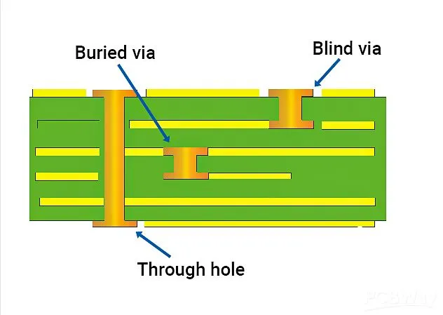
Rigid PCB via types form the foundation of interlayer connectivity, each offering distinct advantages in terms of length, capacitance, and inductance. Through-hole vias, or plated through-holes, extend fully from one board surface to the opposite, providing robust mechanical strength but introducing longer inductive paths that degrade high-frequency signals. Blind vias connect an outer layer to an inner layer without penetrating the entire board thickness, reducing stub length and associated inductance compared to through-hole types. Buried vias link inner layers exclusively, minimizing surface disruption and further shortening the via barrel for better signal integrity in dense designs.
Microvias, often laser-drilled with diameters under 150 microns, enable even tighter spacing and lower parasitics, though they demand advanced fabrication capabilities aligned with standards like IPC-6012 for rigid boards. The choice of rigid PCB via types depends on layer count, routing density, and frequency requirements, with through-hole vias suiting lower-speed power distribution and blind or buried types preferred for critical signal paths. Each type impacts rigid PCB via inductance differently: shorter vias inherently exhibit less inductance due to reduced loop area. Designers evaluate trade-offs in cost, reliability, and performance when selecting via types during initial stackup planning.
The Physics of Rigid PCB Via Inductance and Its Impact on Signal Integrity
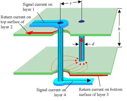
Via inductance arises primarily from the magnetic field generated around the current-carrying barrel, modeled approximately as a coaxial transmission line where inductance scales with barrel length and inversely with diameter. In rigid PCBs, partial inductance dominates at transitions, creating impedance discontinuities that reflect signals, especially when rise times approach or exceed the via's electrical length. This rigid PCB via inductance manifests as ringing or overshoot in time-domain reflectometry, distorting eye diagrams and increasing bit error rates in serial links. Capacitive parasitics from pads and anti-pads compound the issue, altering characteristic impedance and exacerbating crosstalk between adjacent vias.
Signal integrity suffers most in high-speed designs where via stubs act as resonators, trapping energy and radiating electromagnetic interference. Ground bounce from power vias with high inductance further couples noise into signal nets, violating timing margins. Quantifying rigid PCB via inductance requires considering plating thickness, dielectric properties, and return path proximity, with simulations validating empirical models. Adhering to IPC-2221 guidelines ensures vias contribute minimally to overall channel loss.
At frequencies above 1 GHz, via inductance exceeds trace inductance per unit length, shifting design focus to via optimization. Engineers mitigate this by arraying vias or integrating ground return vias nearby, forming low-inductance paths. Understanding these mechanisms allows proactive rigid PCB via design to preserve waveform fidelity across the stackup.
Key Mechanisms Causing Via-Related Signal Degradation
Impedance mismatch at via transitions stems from abrupt changes in geometry, where the via barrel's lower capacitance relative to microstrip or stripline causes step-up reflections. Crosstalk arises when aggressive via fields couple magnetically or capacitively to neighboring structures, amplified by sparse ground planes. Stub effects in through-hole vias create resonant notches in frequency response, attenuating harmonics critical for fast edges.
Return path discontinuities exacerbate rigid PCB via inductance, as signals seek the lowest impedance loop, often detouring through distant planes. Thermal expansion mismatches in multilayer rigid PCBs can shift via positions, altering parasitics over temperature cycles. Fabricators control these via IPC-6012 specifications for plating uniformity and hole wall integrity, preventing voids that increase resistance and inductance.
Best Practices for Minimizing Rigid PCB Via Inductance
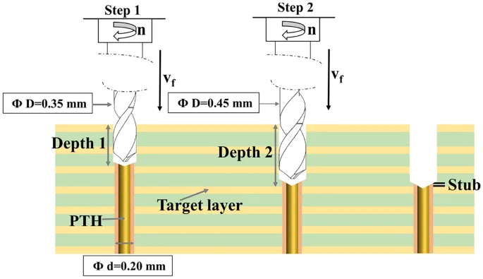
Selecting appropriate rigid PCB via types is the first step: prioritize blind and buried vias to eliminate unnecessary stubs, confining interconnect length to active layers. For through-hole vias unavoidable in mechanical vias or BGA escape routing, implement backdrilling to remove unused barrel segments, reducing effective height by up to 70 percent in thick boards. Smaller drill diameters lower inductance logarithmically, but balance with aspect ratio limits typically under 10:1 for reliable plating.
Parallel via arrays dramatically cut equivalent inductance by distributing current, ideal for power and ground nets; place pairs or fences within 100-200 microns of signal vias to tighten return loops. Filled or plugged vias encapsulate the barrel in conductive epoxy, minimizing air voids and providing smoother impedance profiles for high-current paths. Ground stitching vias along board edges and cutouts ensure continuous reference planes, suppressing slotline modes.
Layout strategies further enhance rigid PCB via signal integrity: position signal vias equidistant from planes, avoiding splits, and fanout high-speed pins with minimal vias. Controlled depth routing for blind vias demands precise process control per IPC standards. Simulate via S-parameters early, tuning pad sizes and anti-pad clearances to match trace impedance, typically 50 or 100 ohms.
Optimizing Via Placement and Spacing for Signal Integrity
Via-to-via spacing prevents coupling: maintain at least three times the largest diameter to limit near-end crosstalk below -30 dB. Surround high-speed vias with ground via shields, forming cages that confine fields and stabilize impedance. In dense BGAs, staggered via grids distribute inductance evenly across power domains.
Layer transitions demand symmetry: align signal, ground, and power vias vertically where possible to preserve broadside coupling. Decoupling capacitors near via fields bypass high-frequency currents, shunting inductance. These rigid PCB via design techniques collectively yield cleaner eye openings and lower jitter.
Troubleshooting Common Via Issues in High-Speed Designs
Engineers often encounter excessive insertion loss from elongated vias in 20+ layer rigid PCBs; backdrilling or transitioning to HDI-style microvias resolves this. Overshoot from inductive vias responds to series resistors or RC networks at drivers, though redesigning the via is preferable. Fabrication anomalies like dog-boning increase resistance; specify tenting and plating per standards.
Field measurements using TDR reveal stub locations, guiding iterative fixes. Case in point: a 10 Gbps SerDes channel improved eye height by 20 percent via blind via substitution and ground shielding, without altering stackup.
Conclusion
Effective rigid PCB via design hinges on selecting via types that minimize barrel length, employing backdrilling and arrays to slash inductance, and strategic placement for robust signal integrity. These practices align electrical performance with manufacturability, ensuring reliable high-speed operation. By integrating IPC-guided principles, engineers avoid common pitfalls like reflections and crosstalk. Prioritize simulation and DFM reviews to validate designs early. Ultimately, thoughtful via optimization elevates rigid PCB performance across demanding applications.
FAQs
Q1: What are the main rigid PCB via types and their impact on inductance?
A1: Rigid PCB via types include through-hole, blind, buried, and microvias. Through-hole vias have the highest rigid PCB via inductance due to full-board traversal and stubs. Blind and buried types reduce length for lower inductance, while microvias offer minimal parasitics in high-density areas. Selection depends on stackup and speed requirements for optimal signal integrity.
Q2: How does rigid PCB via inductance affect signal integrity?
A2: Rigid PCB via inductance introduces discontinuities, causing reflections and overshoot in high-speed signals. It disrupts impedance matching, leading to eye closure and increased jitter. Mitigation through shorter vias and parallel arrays preserves waveform quality. Simulations quantify these effects for proactive design.
Q3: What are best practices for rigid PCB via design to maximize signal integrity?
A3: Key rigid PCB via design practices include using blind/buried vias, backdrilling through-holes, and adding ground stitching. Maintain proper spacing and symmetry for low crosstalk. Align with IPC-2221 for sizing and IPC-6012 for fabrication reliability. These ensure minimal rigid PCB via inductance and clean signals.
Q4: How can engineers reduce rigid PCB via inductance in multilayer boards?
A4: Reduce rigid PCB via inductance by minimizing via length with blind types, employing multiple parallel vias for power/ground, and backdrilling stubs. Place return path vias close to signals. Filled vias and shielding further lower parasitics. Validate with S-parameter analysis for high-frequency integrity.
References
IPC-2221B — Generic Standard on Printed Board Design. IPC, 2009
IPC-6012E — Qualification and Performance Specification for Rigid Printed Boards. IPC, 2017
IPC-4761 — Classification for Microvia-Based (IPC-6012-HDI) and Conventional Rigid Board Plated Through-Hole Barrel Protection. IPC, 2022