Introduction
High-speed digital printed circuit boards handle signals at gigabit-per-second rates, where even minor routing imperfections can lead to significant performance issues. Signal degradation manifests as reflections from impedance discontinuities, crosstalk between adjacent traces, and timing skew that disrupts data integrity. Proper routing techniques form the backbone of signal integrity in these designs, directly impacting eye diagram quality and bit error rates. This article delves into high-speed PCB routing rules, focusing on trace length matching, differential pair routing, via minimization, ground plane routing, serpentine routing, and controlled impedance routing. Engineers applying these methods can achieve robust designs that support advanced protocols like PCIe, USB, and DDR memory interfaces. Mastering these strategies requires a blend of theoretical understanding and practical implementation.
Why Signal Degradation Occurs in High-Speed PCBs
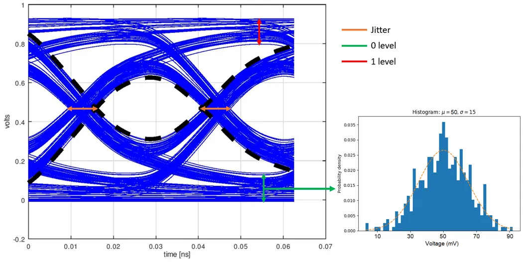
Signal degradation in high-speed PCBs arises primarily from electromagnetic interactions that distort waveforms as they propagate along traces. At frequencies above 1 GHz, transmission line effects dominate, turning PCB traces into waveguides susceptible to reflections when characteristic impedance mismatches occur. Crosstalk coupling between parallel traces introduces noise, while ground bounce from simultaneous switching exacerbates voltage fluctuations. Attenuation increases with frequency due to skin effect and dielectric losses, further narrowing signal margins. These phenomena collectively degrade eye opening and increase jitter, potentially causing system failures. Understanding these root causes is essential before applying targeted routing solutions.
Fundamental Principles of High-Speed Signal Propagation
Transmission line theory governs high-speed signal behavior, where traces must be treated as controlled impedance lines rather than simple wires. The characteristic impedance Z0 depends on trace geometry, substrate properties, and surrounding fields, typically targeted at 50 ohms for single-ended or 100 ohms for differential signals. Reflections occur at impedance steps, quantified by the reflection coefficient Gamma equals (Z2 minus Z1) over (Z2 plus Z1). Propagation delay per unit length varies with effective dielectric constant, influencing skew in multi-trace nets. Return currents flow through the nearest ground plane, making its continuity critical for low inductance loops. These principles underpin all effective routing techniques.
Controlled Impedance Routing
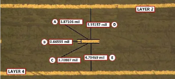
Controlled impedance routing ensures traces maintain a consistent Z0 throughout their length to prevent reflections. Engineers calculate trace width, spacing, and layer stackup using field solver tools based on material epsilon_r and thickness. Microstrip traces on outer layers offer easier fabrication but higher radiation, while striplines embedded between planes provide better shielding at the cost of via transitions. IPC-2221C outlines generic requirements for conductor dimensions and spacing to achieve predictable impedance in printed board designs. Tolerances of plus or minus 10 percent suffice for most applications, but tighter control benefits ultra-high speeds. Verification through time-domain reflectometry confirms design intent post-fabrication.
Ground Plane Routing Strategies
A solid ground plane directly beneath signal traces minimizes loop inductance and provides a low-impedance return path. Splitting planes under high-speed signals introduces impedance variation, so continuous pours are preferred unless isolation demands otherwise. Stitch vias around plane splits connect multiple planes, reducing inductance in return paths. Ground plane routing also suppresses crosstalk by screening fields between layers. Partial fills or hatched planes can balance current handling with field confinement in power-ground combos. Adhering to these practices aligns with performance specifications in standards like IPC-6012E for rigid printed boards.
Via Minimization Techniques
Vias introduce parasitic inductance and capacitance, causing signal reflections and insertion loss, especially at multi-gigahertz frequencies. Minimize via count by optimizing component placement to keep signals on fewer layers, routing horizontally on signal layers and vertically only when necessary. Use blind or buried vias in multilayer boards to avoid through-hole stubs that resonate at quarter-wave frequencies. Via minimization reduces transition discontinuities, improving return loss by several dB. Back-drilling removes stubs in longer vias, though it adds cost and process complexity. Pair vias with nearby ground vias to maintain impedance and shield transitions.
Differential Pair Routing Essentials
Differential pair routing transmits signals as complementary pairs, rejecting common-mode noise and enabling higher data rates. Maintain constant spacing between the positive and negative traces, typically 2 to 3 times the trace width, to achieve target differential impedance. Avoid sharp bends by using smooth 45-degree arcs or curved paths, preventing intra-pair skew. Route pairs tightly coupled over uniform reference planes, eschewing splits or edges. Length matching within the pair, often to within 5 mils, ensures balanced propagation delays. This technique excels in LVDS, SerDes, and Ethernet links.
Trace Length Matching Methods
Trace length matching equalizes propagation delays across signals in parallel buses like address lines or data lanes, minimizing skew-induced errors. Intra-pair matching for differentials prevents mode conversion, while inter-lane matching in multi-lane buses like PCIe preserves timing budgets. Deskew requires tuning longer traces to match the shortest, using meanders or trombones without introducing excessive loss. Simulate phase differences pre-layout to predict required adjustments. Tolerance depends on bit time, often 10 percent of unit interval for gigabit speeds. Proper execution enhances setup and hold margins.
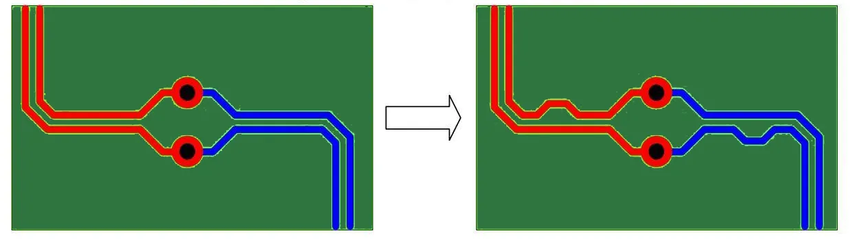
Serpentine Routing for Length Tuning
Serpentine routing employs S-shaped meanders to incrementally lengthen traces for matching without widening the footprint. Design serpentine amplitude and pitch to avoid coupling between adjacent loops, typically spacing loops at least 3 times trace width. Orient loops perpendicular to the routing direction to minimize crosstalk. This method suits dense boards where straight trombones consume space. Control bend radii to prevent radiation, aiming for smooth curves over sharp corners. Serpentine patterns prove invaluable in DDR memory interfaces requiring byte-lane matching.
Integrating Techniques for Optimal Performance
Combine these methods holistically: start with stackup for impedance, place components for short paths, then route with length rules enforced. Use length-tuning features during interactive routing, verifying with post-layout simulations for S-parameters and crosstalk. Ground stitching and decoupling caps support routing integrity. Iterate based on hyperlynx or similar analysis for eye diagrams. Fabricate prototypes with impedance test coupons for correlation. These integrated high-speed PCB routing rules yield designs robust across process variations.
Common Pitfalls and Troubleshooting
Engineers often overlook via stub effects, leading to unexpected resonances; simulate frequency-dependent behavior to identify. Overly aggressive length tuning introduces attenuation from extra trace length and bends. Plane voids under traces cause return path detours, inflating inductance; inspect with 3D field solvers. Fabricated boards failing signal integrity tests may need routing revisions or stackup tweaks. Systematic verification catches issues early. Troubleshooting logs timing violations to root causes like skew or impedance.
Conclusion
Mastering routing techniques like controlled impedance, differential pairs, length matching, via minimization, ground planes, and serpentine patterns minimizes signal degradation in high-speed digital PCBs. These high-speed PCB routing rules preserve waveform integrity, reduce EMI, and ensure compliance with timing budgets. Logical application grounded in transmission line principles delivers reliable performance. Engineers should prioritize simulation and verification to bridge design and reality. As data rates climb, these strategies remain foundational for next-generation boards. Invest time in upfront planning for downstream success.
FAQs
Q1: What are the key high-speed PCB routing rules for minimizing signal degradation?
A1: High-speed PCB routing rules emphasize controlled impedance to prevent reflections, constant ground referencing for low inductance, and minimal vias to reduce parasitics. Maintain trace spacing to limit crosstalk, enforce length matching for skew control, and use differential routing for noise immunity. Adhere to layer stackup planning early. These practices align with industry standards, ensuring gigabit signals propagate cleanly. Simulation verifies compliance before fabrication.
Q2: How does trace length matching improve high-speed PCB performance?
A2: Trace length matching synchronizes signal arrival times across buses or pairs, eliminating skew that closes timing windows. Techniques like serpentine meanders adjust lengths precisely without excess loss. Target tolerances based on bit period, typically under 10 percent. This prevents data errors in DDR or PCIe interfaces. Post-layout checks confirm effectiveness through delay calculations.
Q3: Why is differential pair routing critical in high-speed designs?
A3: Differential pair routing leverages balanced signals for common-mode rejection, boosting noise margins at high speeds. Consistent intra-pair spacing and length matching preserve impedance and phase alignment. Route over solid planes to shield and return currents. Avoid discontinuities that convert modes. This method supports protocols demanding low BER.
Q4: What role does via minimization play in controlled impedance routing?
A4: Via minimization cuts inductive stubs that degrade impedance continuity and cause reflections. Prefer blind vias or back-drilling to shorten paths. Ground via fencing maintains shielding at transitions. Fewer layer changes keep signals in optimal environments. This sustains Z0 tolerance across the board.
References
IPC-2221C — Generic Standard on Printed Board Design. IPC, 2023
IPC-6012E — Qualification and Performance Specification for Rigid Printed Boards. IPC, 2017