Introduction
Rigid-flex printed circuit boards integrate rigid and flexible sections into a single unit, enabling compact designs for applications in medical devices, aerospace, and consumer electronics. Sequential lamination emerges as a critical manufacturing technique for these boards, allowing builders to construct multilayer stackups in stages rather than a single press cycle. This approach accommodates the differing material properties between rigid substrates like FR4 and flexible polyimide films. Engineers must navigate specific rigid-flex PCB design rules to ensure reliability during flexible PCB manufacturing. Sequential lamination challenges arise from thermal and mechanical stresses across multiple cycles. Understanding these elements helps optimize performance and yield.
What Is Sequential Lamination in Rigid-Flex PCBs and Why It Matters
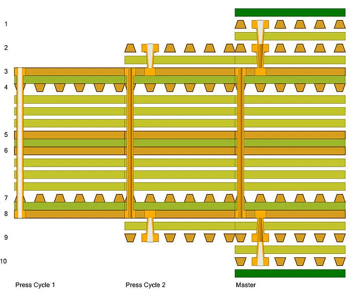
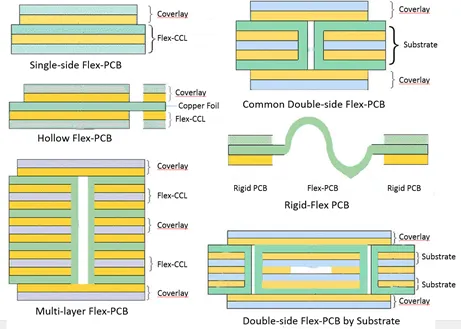
Sequential lamination involves building the PCB through multiple bonding cycles, where subsets of layers are preprocessed, laminated individually, and then joined with prepregs. In rigid-flex boards, flex layers receive coverlay encapsulation first, while rigid layers get adhesion-promoting treatments like brown oxide coating. This staged process supports complex configurations, such as varying flex layer counts between rigid sections or air-gap constructions for enhanced bendability. Factory teams rely on it for high-density interconnects with blind and buried vias, which single-step lamination cannot achieve reliably.
The technique matters because rigid-flex designs demand space savings and mechanical flexibility without sacrificing electrical performance. It enables symmetrical or asymmetrical stackups tailored to impedance needs or via aspect ratios. Without sequential lamination, manufacturers face limitations in layer count and interconnect density, especially in transition zones between rigid and flex areas. Adhering to rigid-flex PCB design rules during this process minimizes sequential lamination challenges, ensuring boards meet dynamic flexing requirements in real-world use. Overall, it drives innovation in compact electronics while aligning with production scalability.
Technical Principles of Sequential Lamination
The core principle centers on controlled bonding under heat and pressure, typically 250 psi adjusted for panel area, to melt and cure prepreg epoxy between layer subsets. Alignment pins maintain registration across cycles, crucial as polyimide flex materials exhibit dimensional instability compared to rigid cores. Each cycle includes drilling, plating, and etching on subsets before final integration, with resin flow filling vias for adhesion. In rigid-flex, plasma cleaning prepares flex surfaces, while rigid layers ensure uniform prepreg sheets by routing out flex areas beforehand.
Coefficient of thermal expansion (CTE) differences dominate the mechanics, with resins expanding far more than copper above glass transition temperature (Tg), risking delamination if materials mismatch. Z-axis expansion during pressing can create voids or squeeze resin outward, altering stackup thickness. Multiple cycles amplify these effects, as cumulative shrinkage demands scaling adjustments in design files for accurate registration. Factories monitor Tg above 180 degrees C and low Z-axis CTE below 70 ppm per degree C in dielectrics to mitigate stresses.

Rigid-Flex PCB Design Rules for Sequential Lamination
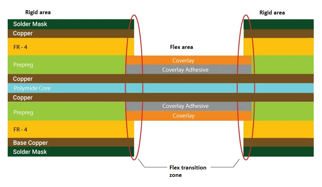
Designers must prioritize symmetrical constructions in rigid sections for warp resistance, centering flex layers to balance stresses. Transition zones require isolation routing or hatched copper patterns to avoid strain concentration, preventing cracks during bends per IPC-2223 guidelines. Minimum bend radii follow IPC-2223 standards, typically 10 times the flex section thickness, with thinner copper foils enhancing fatigue life. Vias demand staggered placement and teardrops on pads to handle plating stresses, avoiding high-flex regions altogether.
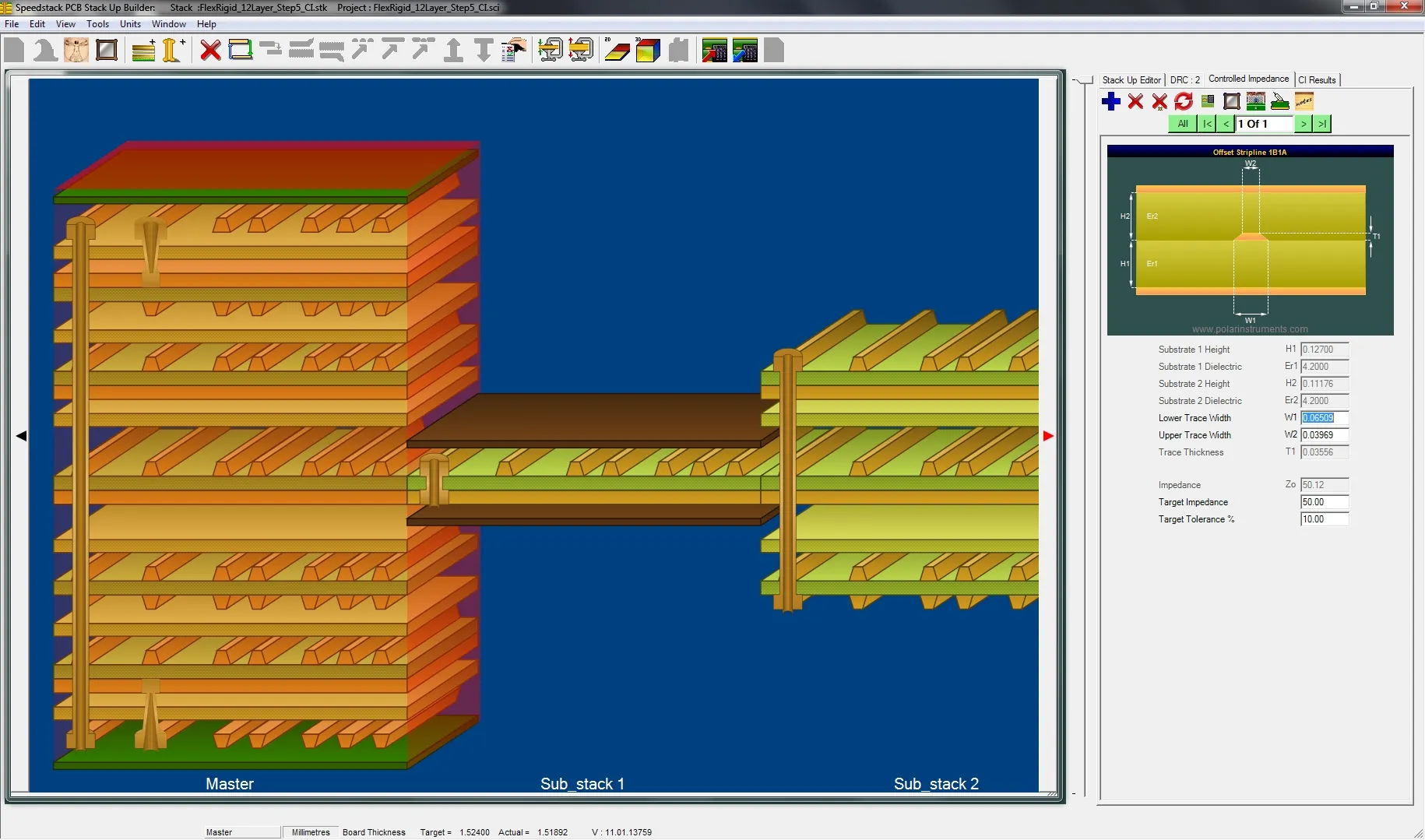
Stackup planning limits sequential cycles to two or three, as more increase misalignment risks and costs. Air-gap designs separate flex pairs without adhesives in rigid areas, improving flexibility for four or more flex layers while meeting IPC-2223 criteria. Impedance control spans zones using ground planes, with odd-layer counts enabling stripline routing for RF integrity. Engineers specify high-Tg, low-CTE laminates compatible across materials to support these rules during flexible PCB manufacturing.
Material selection emphasizes polyimide for flex durability and FR4 prepregs tailored for rigid-flex bonding. Blind vias in rigid areas require aspect ratios feasible for mechanical drilling, typically under 10:1. Procurement teams communicate fab limits on trace widths and via sizes early to embed margins.
Manufacturing Challenges in Sequential Lamination for Flexible PCB Manufacturing
Sequential lamination challenges peak with CTE mismatches, causing warpage as flex polyimide shifts differently from rigid cores under thermal cycling. Multiple laminations induce dimensional changes, complicating drill alignment from Gerber files and raising scrap rates. Resin squeeze-out disrupts uniform thickness, while voids form if prepreg flow fails into blind vias, per observations in high-cycle builds.
Layer registration falters beyond three cycles due to cumulative tolerances, especially with asymmetrical stackups needing fixtures. Aspect ratios limit via reliability, as deeper holes in thicker rigid sections strain plating uniformity. Factories encounter higher costs from extended lead times, multi-day processes, and rework for delamination in transition zones.
Adhesion issues arise without proper surface treatments, with brown oxide on rigid and plasma on flex proving essential yet sensitive to handling. Z-axis inconsistencies affect final bow and twist, failing IPC-6013 qualification for flexible boards. These hurdles demand tight process controls in flexible PCB manufacturing.
Best Practices and Troubleshooting for Sequential Lamination
Limit cycles to two or three, optimizing stackups to minimize vias and layers without compromising density. Select laminates per IPC-4101 with consistent flow and Tg stability across cycles, pairing low-CTE polyimides with matched rigid prepregs. Use alignment pins religiously and scale panels for shrinkage in design software.
For troubleshooting, inspect transitions with cross-section analysis for voids or misalignment post-first cycle. Mitigate warpage via gradual cooling and hold-down fixtures during pressing. Plasma cleaning and oxide treatments ensure bonding; test adhesion pulls early.
Incorporate stiffeners only where needed, laminating them separately to avoid bulk. Ground planes shield EMI across zones, with hatched patterns relieving flex stress. These practices align factory outputs with IPC-6013 performance specs.
Conclusion
Sequential lamination unlocks advanced rigid-flex capabilities but demands vigilant rigid-flex PCB design rules to counter inherent sequential lamination challenges. By matching materials, limiting cycles, and following standards like IPC-2223, engineers achieve reliable flexible PCB manufacturing. Factories gain from structured processes that balance complexity with yield. Prioritizing transitions and CTE harmony ensures boards withstand flexing and thermal loads. Ultimately, these insights empower designs that perform in demanding environments.
FAQs
Q1: What are the primary rigid-flex PCB design rules for sequential lamination?
A1: Key rules include symmetrical rigid stackups, isolation routing in transitions, and bend radii per IPC-2223 at least 10 times flex thickness. Avoid vias in high-flex areas and stagger them in rigid sections for plating reliability. Limit cycles to 2–3, using air-gaps for multi-layer flex. These prevent warpage and delamination during manufacturing.
Q2: What sequential lamination challenges impact flexible PCB manufacturing most?
A2: CTE mismatches cause warpage and voids, while multiple cycles risk misalignment and resin squeeze-out. Registration issues from polyimide instability demand precise alignment pins. Aspect ratio limits via drilling in thick rigid areas. Factories troubleshoot with surface treatments and controlled pressing to maintain IPC-6013 compliance.
Q3: How does sequential lamination differ in rigid-flex versus standard rigid PCBs?
A3: Rigid-flex requires staged coverlay on flex first, brown oxide on rigid, and tailored prepregs with flex cutouts. Challenges amplify from material differences, needing plasma cleaning for adhesion. It supports varying flex counts unlike uniform rigid builds. This enables compact, bendable designs aligned with factory processes.
Q4: What best practices mitigate warpage in rigid-flex sequential lamination?
A4: Choose low-CTE, high-Tg materials per IPC-4101 and cool gradually post-press. Use fixtures for asymmetrical stacks and scale Gerbers for shrinkage. Inspect subsets between cycles for voids. These steps ensure uniform Z-axis control and high yields in production.
References
IPC-2223 — Sectional Design Standard for Flexible Printed Boards. IPC
IPC-6013 — Qualification and Performance Specification for Flexible Printed Boards. IPC
IPC-4101 — Specification for Base Materials for Rigid and Flexible Printed Boards. IPC