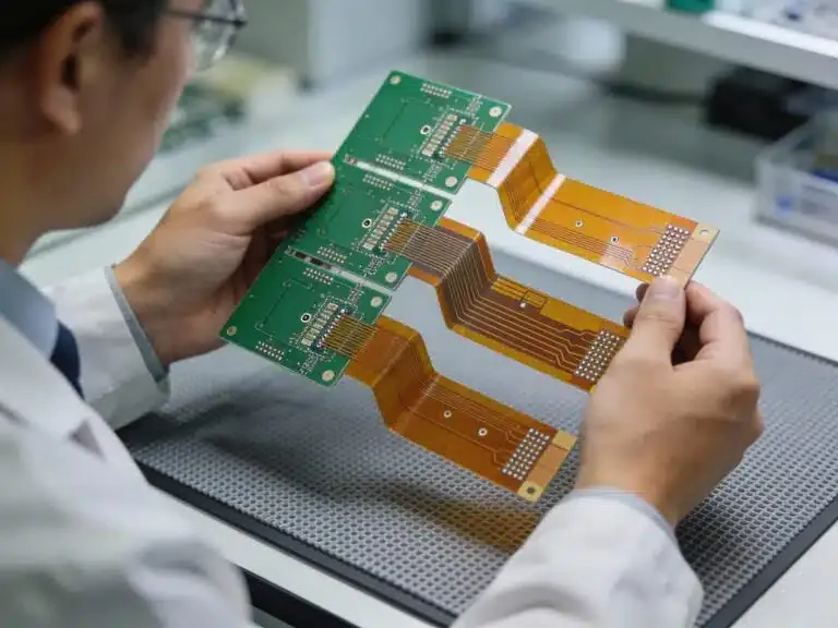
Introduction
In high-speed PCB designs, signal integrity challenges arise as data rates climb into the gigahertz range, demanding precise control over every layout element. Engineers face issues like crosstalk, reflections, and impedance mismatches that degrade performance and lead to system failures. Minimum trace spacing emerges as a critical parameter, directly influencing electromagnetic coupling between adjacent traces and maintaining signal quality. This article explores pcb trace spacing signal integrity principles, focusing on minimum trace spacing for differential pairs and impedance control trace spacing strategies. By optimizing these factors, designers achieve reliable high-speed pcb layout guide outcomes. Understanding these relationships enables engineers to balance density with performance in multilayer boards.
Understanding Signal Integrity in PCB Design
Signal integrity refers to the preservation of electrical signal quality from transmitter to receiver, encompassing amplitude, rise time, and timing accuracy. Poor signal integrity manifests as overshoot, ringing, or eye diagram closure, compromising data transmission in applications like SerDes or DDR memory interfaces. Trace spacing plays a pivotal role by minimizing unwanted interactions between signals, such as near-end and far-end crosstalk. In dense layouts, insufficient spacing amplifies capacitive and inductive coupling, leading to noise injection that propagates through the board. Engineers must consider not only intra-layer spacing but also inter-layer clearances in stackups. Proper spacing ensures signals remain clean, supporting higher frequencies without additional mitigation like shielding.
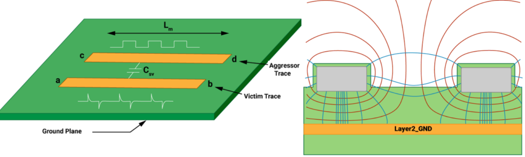
The Role of Minimum Trace Spacing in Crosstalk Mitigation
Crosstalk occurs when electromagnetic fields from an aggressor trace induce voltage or current in a victim trace, with coupling strength inversely proportional to spacing. Capacitive crosstalk dominates at close spacings due to fringing fields between edges, while inductive crosstalk arises from mutual inductance in parallel runs. Minimum trace spacing guidelines help establish safe distances, typically scaling with trace width and dielectric properties. For single-ended signals, spacing greater than three times the trace width reduces coupling below acceptable thresholds in most scenarios. In high-speed designs, dynamic effects like simultaneous switching noise further underscore the need for generous clearances. By adhering to these principles, pcb trace spacing signal integrity improves, preventing bit errors in critical paths.
Impedance Control and Trace Spacing Relationships
Characteristic impedance of a trace depends on its width, thickness, height above reference plane, and spacing to adjacent traces. Closely spaced traces alter the effective dielectric field distribution, lowering impedance due to increased capacitance. Impedance control trace spacing becomes essential for controlled impedance lines, where tolerances of 10% or tighter are common in high-speed applications. Engineers calculate spacing using field solver approximations or empirical formulas, ensuring pairs maintain target values like 50 ohms single-ended or 100 ohms differential. Variations in spacing along a trace length introduce return path discontinuities, exacerbating reflections. Consistent spacing preserves impedance profile, aligning transmitted and received waveforms effectively.
Minimum Trace Spacing for Differential Pairs
Differential pairs carry balanced signals across two traces, rejecting common-mode noise through subtraction at the receiver. Minimum trace spacing for differential pairs must balance intra-pair tightness for low common-mode impedance with inter-pair separation to avoid skew-induced crosstalk. Intra-pair spacing, often equal to trace width, minimizes loop area and inductance imbalance. Inter-pair spacing, ideally five to ten times the intra-pair gap, suppresses coupling between adjacent pairs. Edge-coupled microstrips on outer layers demand wider separations than broadside-coupled in inner layers due to stronger fringing fields. IPC-2221B provides foundational guidelines for conductor spacing based on voltage and current, adaptable for signal integrity in high-speed contexts.
Factors Influencing Trace Spacing Decisions
Dielectric materials, layer count, and routing topology all modulate effective spacing requirements. Thinner dielectrics increase field coupling, necessitating wider traces or greater separations to maintain impedance. Via transitions and bends introduce discontinuities, where local spacing adjustments prevent resonance. Board thickness and copper weight also factor in, as heavier copper widens effective trace edges. Temperature and humidity variations expand or contract materials, subtly shifting spacings over time. Engineers simulate these interactions early, iterating layouts to meet timing budgets.
Best Practices for High-Speed PCB Layout
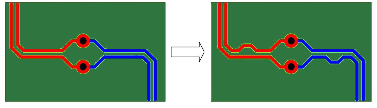
Start with a robust stackup design, placing high-speed signals between ground planes for tight field containment. Route differential pairs with length matching within 5 mils over their entire length to avoid skew. Maintain uniform spacing by using routing grids aligned to design rules, avoiding acute angles that concentrate fields. For impedance control trace spacing, verify with 2D field solvers during routing. IPC-6012E outlines performance specs for rigid boards, emphasizing conductor definition that supports precise spacing control. Incorporate guard traces or stitching vias sparingly, as they can introduce new coupling paths if not spaced properly.
Common Pitfalls and Troubleshooting Strategies
Overly aggressive spacing savings lead to crosstalk floors that mask other issues, complicating debug. Measure eye diagrams post-layout simulation to quantify coupling effects. If crosstalk exceeds 1% of signal amplitude, widen spacings incrementally and recheck. Fanout patterns from BGA packages demand radial spacing increases to dilute density. Power plane splits create return path detours, amplifying effective coupling distances. Systematic review of length-matched nets ensures phase alignment across pairs.
Advanced Considerations for Multi-Gigabit Designs
At data rates beyond 10 Gbps, skin effect and dielectric loss join spacing concerns, but baseline separations remain foundational. SerDes channels benefit from asymmetric spacing to neighbors, prioritizing quiet references. Backdrilling vias reduces stubs that reflect into spacing-sensitive regions. Pre-emphasis and equalization compensate residuals, but optimal pcb trace spacing signal integrity reduces reliance on these. Layer transitions via blind vias preserve spacing continuity. High-speed pcb layout guide emphasizes holistic optimization over isolated fixes.
Conclusion
Optimizing minimum trace spacing stands as a cornerstone of signal integrity in high-speed PCB designs, directly curbing crosstalk and stabilizing impedance. From differential pairs to dense routing arrays, thoughtful spacing decisions enable reliable gigabit performance without excessive board real estate. Engineers armed with principles from standards like IPC-2221B and IPC-6012E can navigate trade-offs confidently. Integrating these practices yields layouts that pass first-pass validation, minimizing respins. As designs push boundaries, disciplined spacing remains a timeless engineering lever for success.
FAQs
Q1: What factors determine pcb trace spacing signal integrity requirements?
A1: Pcb trace spacing signal integrity hinges on crosstalk types, impedance targets, and frequency content. Capacitive coupling drops rapidly with spacing beyond three times trace width, while inductive effects persist over longer distances. Dielectric constant and reference plane proximity modulate these, demanding simulation for precision. Standards like IPC-2221B offer baseline voltage-based spacings adaptable to high-speed needs. Always verify with time-domain reflectometry for real-world validation.
Q2: How do you calculate minimum trace spacing for differential pairs?
A2: Minimum trace spacing for differential pairs starts with intra-pair gap matching trace width for balance, then inter-pair separation of five to ten times that to curb crosstalk. Field solvers compute exact values based on stackup height and materials. Aim for 100-ohm differential impedance with edge coupling on outer layers requiring wider gaps. Length matching within tolerances prevents skew. Simulate aggressor-victim scenarios to confirm noise margins.
Q3: Why is impedance control trace spacing critical in high-speed designs?
A3: Impedance control trace spacing prevents capacitance buildup between neighbors, which lowers characteristic impedance and causes reflections. Uniform spacing maintains 50/100-ohm targets across lengths, preserving waveform integrity. Discontinuities from varying gaps introduce return path shifts, worsening signal distortion. High-speed pcb layout guide stresses consistent routing grids for this. Post-route extraction verifies tolerances under 10%.
Q4: What are common high-speed pcb layout guide tips for trace spacing?
A4: High-speed pcb layout guide prioritizes ground-referenced routing with spacings exceeding three times width for single-ended lines. Differential pairs need tight intra-pair and loose inter-pair gaps. Avoid routing over splits or under power planes. Use grids for uniformity and simulate coupling early. IPC-6012E supports these through conductor quality specs. Balance density with margins for manufacturing tolerances.
References
IPC-2221B — Generic Standard on Printed Board Design. IPC, 2012
IPC-6012E — Qualification and Performance Specification for Rigid Printed Boards. IPC, 2017