Introduction
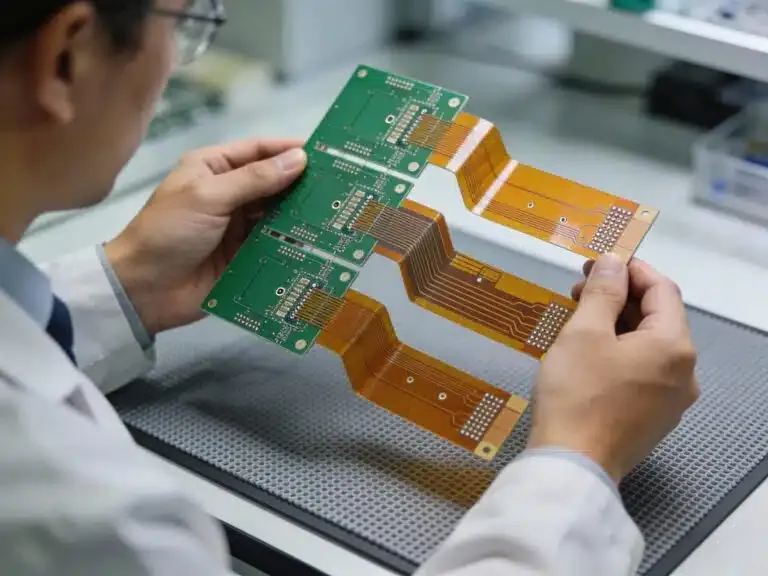
For electronic hobbyists venturing into complex projects, designing an 8-layer PCB can be both exciting and challenging. Signal integrity basics are crucial to ensure that high-speed signals travel without distortion or interference. Issues like crosstalk, signal reflection, and transmission line effects can degrade performance if not addressed. Proper PCB impedance control is essential to maintain signal quality, especially in multilayer designs. This article aims to simplify these concepts for hobbyists, offering practical tips to reduce crosstalk and achieve reliable designs. Whether you are building a high-speed digital circuit or a mixed-signal system, understanding these principles will elevate your PCB projects. Let's explore how to tackle signal integrity challenges with actionable advice tailored for an 8-layer PCB layout.
What Is Signal Integrity and Why It Matters
Signal integrity refers to the quality of an electrical signal as it travels through a PCB. It ensures that the signal remains undistorted and free from noise or interference. In high-speed designs, poor signal integrity can lead to data errors, timing issues, or complete system failure. For hobbyists working on 8-layer PCBs, signal integrity basics become even more critical due to the increased complexity of routing and layer stacking. These designs often handle faster signals and denser layouts, making them prone to problems like crosstalk and signal reflection. Addressing transmission line effects and maintaining PCB impedance control can prevent performance issues. By prioritizing signal integrity, hobbyists can build reliable circuits that function as intended, saving time and effort in troubleshooting.
Technical Principles of Signal Integrity in 8-Layer PCBs
Understanding Transmission Line Effects
Transmission line effects occur when signal wavelengths approach the length of PCB traces. At high frequencies, traces act as transmission lines, and mismatches in impedance can cause signal reflection. This reflection distorts the signal, leading to errors in data transmission. In an 8-layer PCB, longer traces and multiple layers increase the risk of such effects. Hobbyists must consider the dielectric constant of the board material and trace geometry to minimize these issues. Proper termination techniques can also absorb reflected signals, preserving integrity.
Signal Reflection and Its Impact
Signal reflection happens when a signal encounters an impedance mismatch along its path. This mismatch can occur at connectors, vias, or improperly terminated traces. Reflected signals interfere with the original signal, causing overshoot or ringing. In multilayer designs, managing signal reflection is vital as signals often transition between layers through vias. Uncontrolled reflections degrade signal quality, especially in high-speed applications. Addressing this requires careful PCB impedance control and attention to trace routing.
Crosstalk in Multilayer Designs
Crosstalk is the unwanted coupling of signals between adjacent traces. In an 8-layer PCB, dense routing and proximity of traces heighten the risk of crosstalk. This interference can distort signals, leading to errors in digital circuits. Crosstalk is influenced by trace spacing, layer stackup, and the presence of ground planes. Reducing crosstalk involves strategic layout planning to isolate sensitive signals. Hobbyists must prioritize spacing and shielding to maintain signal integrity in complex designs.
Importance of PCB Impedance Control
PCB impedance control ensures that traces maintain a consistent characteristic impedance. This consistency prevents signal reflection and supports clean signal transmission. In high-speed designs, impedance mismatches can cause significant signal distortion. For an 8-layer PCB, controlling impedance involves selecting appropriate materials and defining trace widths. It also requires attention to the layer stackup to balance signal and ground layers. Proper impedance management is a cornerstone of signal integrity for hobbyists tackling advanced projects.
Suggested Reading: Choosing the Right Components for Your 8 Layer PCB Projects: A Beginner's Guide
Practical Solutions for Better Signal Integrity
Optimize Layer Stackup for Signal Isolation
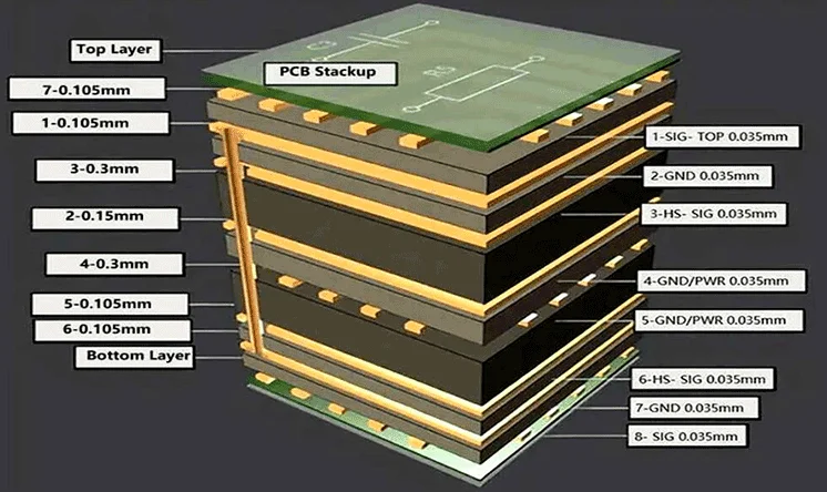
A well-designed layer stackup is the foundation of signal integrity in an 8-layer PCB. Place ground planes adjacent to signal layers to provide shielding and reduce crosstalk. A common approach is to alternate signal and ground layers, ensuring each signal layer has a nearby reference plane. For example, dedicate inner layers to power and ground distribution while routing high-speed signals on outer layers. This setup minimizes interference and supports consistent PCB impedance control. Hobbyists should sketch the stackup early in the design phase to plan signal paths effectively.
Maintain Proper Trace Spacing to Reduce Crosstalk
Reducing crosstalk starts with adequate spacing between traces. Keep high-speed traces apart to limit electromagnetic coupling. A general guideline is to maintain a spacing of at least three times the trace width for critical signals. If space is limited, route sensitive traces on different layers with a ground plane in between. This physical separation acts as a barrier, significantly lowering interference. For hobbyists, using design software to check spacing rules can prevent crosstalk issues before fabrication.
Implement Impedance Control Techniques
Achieving PCB impedance control requires defining trace dimensions based on the desired characteristic impedance. Use online calculators or design tools to determine the correct trace width and spacing for your board's dielectric material. Ensure that the layer stackup supports uniform impedance by maintaining consistent dielectric thickness. Avoid abrupt changes in trace width or routing over split planes, as these disrupt impedance. Hobbyists should verify these parameters during the design review to avoid signal reflection and transmission line effects.
Use Ground Planes Effectively
Ground planes are essential for signal integrity in multilayer PCBs. They provide a low-impedance return path for signals, reducing noise and crosstalk. In an 8-layer design, dedicate at least two layers to continuous ground planes. Avoid routing traces over splits or gaps in the ground plane, as this can lead to signal distortion. Stitch ground planes together with vias around the board's perimeter to create a robust shield. This practice helps hobbyists maintain clean signals in high-speed circuits.
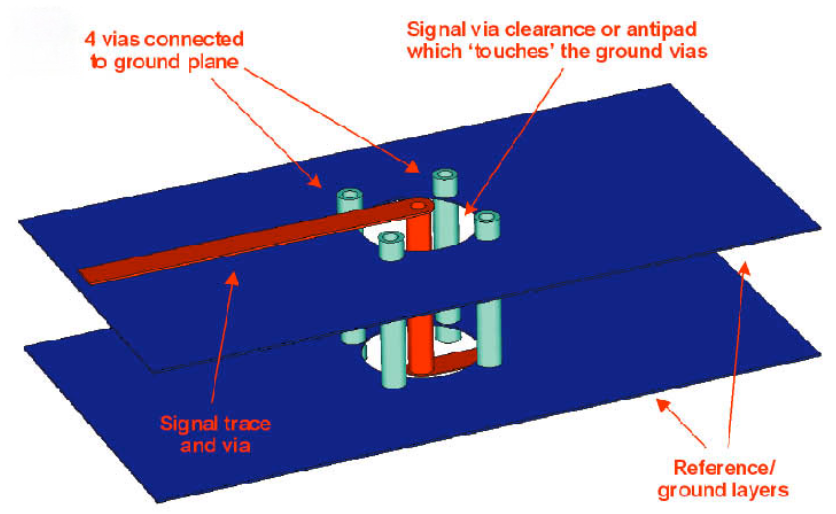
Minimize Via Usage and Optimize Placement
Vias introduce impedance discontinuities and can cause signal reflection. Limit their use in high-speed signal paths by routing traces on a single layer when possible. If vias are unavoidable, place them strategically to minimize stub length, which can act as an antenna for noise. Use back-drilling for critical signals to remove unused via stubs in multilayer designs. Hobbyists should plan via placement early to balance signal integrity with layout constraints.
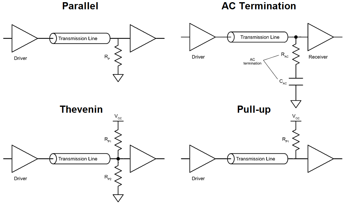
Terminate High-Speed Signals Properly
Proper termination prevents signal reflection by matching the impedance at the end of a transmission line. Common termination methods include series resistors at the source or parallel resistors at the load. Select resistor values based on the characteristic impedance of the trace, often around 50 ohms for high-speed signals. Place termination components close to the signal pins to maximize effectiveness. For hobbyists, experimenting with termination on a prototype can fine-tune performance.
Troubleshooting Signal Integrity Issues
Hobbyists often face signal integrity challenges when testing their 8-layer PCB designs. A common issue is unexpected noise or jitter in high-speed signals, often caused by crosstalk or poor grounding. Start troubleshooting by inspecting the layer stackup for proper ground plane placement. Use an oscilloscope to observe signal waveforms for signs of reflection or ringing. If crosstalk is suspected, review trace spacing and consider rerouting sensitive lines. For impedance mismatches, check trace dimensions against design specifications. Documenting each design iteration helps identify patterns and refine future layouts. Patience and systematic testing are key to resolving these issues without advanced tools.
Conclusion
Mastering signal integrity basics is a game-changer for electronic hobbyists designing 8-layer PCBs. By understanding transmission line effects, signal reflection, and crosstalk, you can prevent common pitfalls in high-speed circuits. Practical steps like optimizing layer stackup, maintaining PCB impedance control, and reducing crosstalk through spacing ensure reliable performance. Implementing ground planes and proper termination further enhances signal quality. With these tips, hobbyists can tackle complex multilayer designs with confidence. Consistent attention to detail during layout and testing transforms challenging projects into successful builds.
FAQs
Q1: What are the key factors affecting signal integrity in 8-layer PCB designs?
A1: Signal integrity in 8-layer PCB designs is influenced by transmission line effects, crosstalk, and signal reflection. Impedance mismatches, poor grounding, and inadequate trace spacing can degrade signal quality. Proper layer stackup with ground planes and controlled impedance are vital. Hobbyists should focus on routing strategies and termination to minimize interference and ensure clean signal transmission in high-speed applications.
Q2: How can hobbyists reduce crosstalk in multilayer PCBs?
A2: Reducing crosstalk in multilayer PCBs involves increasing trace spacing and using ground planes between signal layers. Route sensitive signals on separate layers or maintain a spacing of at least three times the trace width. Stitching ground planes with vias also helps shield signals. Hobbyists can use design software to enforce spacing rules and visually inspect layouts for potential interference.
Q3: Why is PCB impedance control important for high-speed signals?
A3: PCB impedance control is crucial for high-speed signals to prevent signal reflection and ensure clean transmission. Mismatched impedance causes distortions that lead to data errors. Consistent trace dimensions and dielectric properties maintain the desired impedance. Hobbyists should calculate trace widths and verify stackup design to support signal integrity across the board.
Q4: How do transmission line effects impact PCB performance?
A4: Transmission line effects impact PCB performance by causing signal reflection and distortion at high frequencies. When trace lengths approach signal wavelengths, impedance mismatches become significant. This leads to timing issues and data loss in digital circuits. Hobbyists can mitigate these effects with proper termination and impedance control to ensure reliable operation of their designs.
References
IPC-2221B - Generic Standard on Printed Board Design. IPC, 2012.
IPC-6012E - Qualification and Performance Specification for Rigid Printed Boards. IPC, 2020.
IPC-A-600K - Acceptability of Printed Boards. IPC, 2020.