Introduction
For electronic hobbyists venturing into printed circuit board \, understanding signal layers is a fundamental step toward creating functional and reliable projects. Signal layers form the backbone of any PCB, carrying electrical signals between components to ensure proper operation. Whether you are working on simple single-sided PCBs or stepping up to dual-layer PCBs, grasping signal layer basics can significantly improve your designs. This article aims to break down the concept of signal layers, explain their role in PCB design for hobbyists, and provide practical tips for working with simple signal layers. By focusing on foundational knowledge and actionable advice, hobbyists can confidently tackle their first projects while avoiding common pitfalls in signal routing and layer management.
What Are Signal Layers and Why Do They Matter
Signal layers are conductive paths on a PCB that transmit electrical signals between components, such as microcontrollers, resistors, and sensors. In essence, these layers act as the wiring of your circuit, determining how effectively data and power move across the board. For hobbyists, understanding signal layers is crucial because poor routing or layer planning can lead to issues like signal interference, noise, or complete circuit failure.
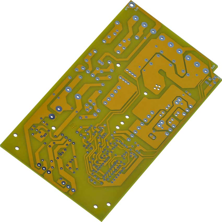
In single-sided PCBs, there is only one conductive layer, typically made of copper, where all traces and components reside. This simplicity makes them ideal for basic projects but limits their capacity for complex circuits. Dual-layer PCBs, on the other hand, offer two conductive layers, usually on both sides of the board, allowing for more intricate designs and better signal management. The choice between single-sided and dual-layer PCBs often depends on the complexity of your project and the need for efficient signal routing.
Signal layers matter because they directly impact signal integrity, which refers to the quality and reliability of electrical signals as they travel through the board. Poorly designed layers can introduce noise or crosstalk, disrupting communication between components. For hobbyists, mastering simple signal layers ensures that even basic designs function as intended, paving the way for more advanced projects.
Related Reading: High Frequency PCB Routing Techniques: Minimizing Signal Loss and Interference
Technical Principles of Signal Layers in PCB Design
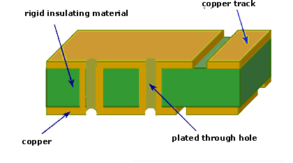
Signal layers are typically made of thin copper foil laminated onto a non-conductive substrate, such as FR-4, a common material in PCB fabrication. The primary principle behind signal layers is to provide a low-resistance path for electrical currents while minimizing interference. In PCB design for hobbyists, this involves careful planning of trace widths, spacing, and layer arrangement to maintain signal integrity.
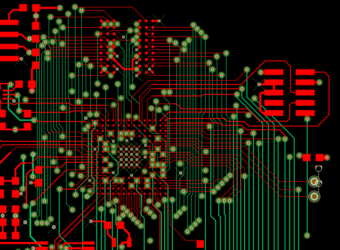
For single-sided PCBs, all signals are routed on one layer, which can lead to crowded traces in more complex designs. This setup often requires jumper wires or creative routing to avoid trace crossings, which can introduce errors if not done carefully. Dual-layer PCBs address this limitation by offering a second layer, allowing traces to cross over each other without interference through the use of vias, which are small conductive holes connecting the layers.
A key concept in signal layer design is impedance, which affects how signals propagate through traces. While hobbyists working on low-speed circuits may not need to calculate impedance, understanding its role becomes important when dealing with faster signals or longer traces. Another principle is avoiding sharp corners in trace routing, as they can cause signal reflection or loss. Instead, use 45-degree angles or smooth curves to maintain signal quality.
Ground planes also play a vital role in signal layers, especially in dual-layer PCBs. A ground plane is a large area of copper connected to the ground, providing a return path for signals and reducing noise. For hobbyists, dedicating one layer of a dual-layer PCB to a ground plane can significantly improve circuit performance, especially in projects involving digital signals or microcontrollers.
Related Reading: Signal Integrity PCB Designers
Practical Tips for Designing Simple Signal Layers
Designing effective signal layers as a hobbyist requires a balance between simplicity and attention to detail. Below are actionable tips tailored for beginners working on single-sided and dual-layer PCBs to ensure reliable performance.
Start with a Clear Schematic
Before laying out signal layers, create a detailed schematic of your circuit. This blueprint helps identify how components connect and where signals need to travel. For single-sided PCBs, plan your layout to minimize trace crossings. If crossings are unavoidable, consider using zero-ohm resistors or jumper wires as a workaround.
Keep Traces Short and Direct
Long traces can introduce delays or noise, especially in high-speed circuits. Aim to keep signal paths as short and direct as possible. In dual-layer PCBs, use vias strategically to switch layers and shorten trace lengths. However, avoid excessive vias, as they can add resistance and complexity.
Separate Power and Signal Traces
To prevent interference, keep power traces separate from signal traces. Power traces often carry higher currents, which can induce noise in sensitive signal lines. In dual-layer PCBs, consider dedicating one layer to power and ground while reserving the other for signals. For single-sided PCBs, maintain adequate spacing between power and signal traces.
Use Ground Planes When Possible
Incorporating a ground plane, especially in dual-layer designs, can reduce noise and improve signal stability. A ground plane acts as a shield, minimizing electromagnetic interference. If a full ground plane is not feasible, create ground pours around critical signal areas to achieve similar benefits.
Follow Trace Width and Spacing Guidelines
Trace width and spacing are critical for maintaining signal integrity and preventing short circuits. For hobbyist projects, wider traces are generally safer for power lines, while narrower traces suffice for low-current signals. Ensure spacing between traces complies with basic design rules to avoid crosstalk. Many free design tools include built-in checks to help with this.
Test and Iterate
After completing your PCB layout, double-check your design for errors. Simulate the circuit if possible, or prototype it on a breadboard to confirm functionality. Once the board is fabricated, test it thoroughly to identify any signal issues. Iteration is key to mastering PCB design for hobbyists, as each project offers learning opportunities.
Common Challenges with Signal Layers for Hobbyists
Hobbyists often encounter specific challenges when working with signal layers, especially when transitioning from single-sided to dual-layer PCBs. One common issue is trace overcrowding in single-sided designs, which can lead to messy layouts or signal interference. To address this, prioritize critical signals and route them first, leaving less important connections for later adjustments.
Another challenge is managing vias in dual-layer PCBs. While vias allow for more flexible routing, improper placement can disrupt signal flow or increase manufacturing complexity. Limit the number of vias and place them close to components to minimize trace length on the opposite layer.
Noise and crosstalk are also frequent concerns, particularly in designs without a proper ground plane. If a ground plane is not an option, ensure adequate spacing between traces and avoid running parallel signal lines for long distances. For digital circuits, adding small decoupling capacitors near power pins of integrated circuits can help filter out noise.
Finally, hobbyists may struggle with selecting the right layer configuration for their project. Single-sided PCBs are cost-effective and simpler to design, making them suitable for basic circuits like LED arrays or simple timers. Dual-layer PCBs, while more complex, are better for projects requiring denser routing, such as microcontroller-based systems. Evaluate your project requirements carefully before deciding on the layer count.
Conclusion
Understanding signal layer basics is an essential skill for electronic hobbyists looking to create functional and reliable PCB designs. By grasping the role of signal layers in single-sided and dual-layer PCBs, beginners can make informed decisions about trace routing, layer configuration, and noise management. Practical steps like starting with a clear schematic, keeping traces short, and using ground planes can significantly enhance the quality of simple signal layers. While challenges like overcrowding or noise may arise, they can be mitigated with careful planning and iterative testing. As hobbyists gain experience with PCB design, these foundational principles will serve as a stepping stone to more complex projects, ensuring consistent performance and learning along the way.
FAQs
Q1: What are the main differences between signal layers in single-sided and dual-layer PCBs?
A1: In single-sided PCBs, signal layers are limited to one conductive surface, making routing simple but restrictive for complex designs. Dual-layer PCBs have two conductive layers, allowing more flexible trace routing with vias to connect sides. This setup supports denser circuits and better signal management, ideal for hobbyists tackling advanced projects while maintaining signal integrity through proper planning.
Q2: How can hobbyists ensure signal integrity in PCB design?
A2: Hobbyists can maintain signal integrity by keeping traces short and direct, using ground planes in dual-layer PCBs, and separating power and signal lines. Avoid sharp trace corners and ensure proper spacing to prevent crosstalk. Testing the design and using decoupling capacitors near critical components also helps reduce noise and ensures reliable performance in simple signal layers.
Q3: What are common mistakes when designing simple signal layers?
A3: A frequent mistake is overcrowding traces on single-sided PCBs, leading to interference or errors. Another is neglecting ground planes in dual-layer designs, increasing noise. Hobbyists often overuse vias, adding complexity, or ignore trace spacing, risking crosstalk. Careful planning and design rule checks can help avoid these pitfalls in PCB design for hobbyists.
References
IPC-2221B — Generic Standard on Printed Board Design. IPC, 2012.
IPC-6012E — Qualification and Performance Specification for Rigid Printed Boards. IPC, 2020.
IPC-A-600K — Acceptability of Printed Boards. IPC, 2020.


