What Are Plated Through-Holes (PTHs) and Why Are They Essential?
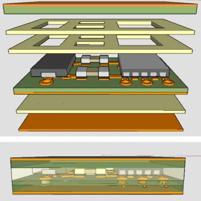
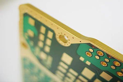
Plated through-holes (PTHs) are fundamental features within a printed circuit board (PCB), serving as conductive pathways that connect different layers of the board. These holes are created by drilling through the PCB material, followed by a plating process that deposits a layer of copper, typically ranging from 20 to 25 micrometers in thickness, to ensure robust electrical connectivity. PTHs are crucial both for mounting traditional through-hole components and for enabling signals to traverse between layers in complex multilayer board designs.
However, imperfections within PTHs can lead to significant issues, including electrical malfunctions, structural weaknesses, and a reduced operational lifespan for the board. Problems such as cracks in the copper barrel, unplated areas (voids), or inadequate connections to internal layers can result in intermittent signal failures or complete circuit breakdown. A thorough understanding and proactive resolution of these defects are paramount for maintaining high PCB performance, especially in demanding sectors like automotive, aerospace, and telecommunications.
Identifying Common Plated Through-Hole Defects and Their Origins
Before delving into resolution strategies, let's examine the most frequently encountered PTH defects, their underlying causes, and their impact on PCB functionality. Early identification of these issues can significantly conserve time and resources during the manufacturing and testing phases.
PTH Barrel Cracks
PTH barrel cracks refer to breaks or fractures within the copper plating that lines the interior of the hole. These fissures commonly develop at corners or along the barrel due to mechanical stress or thermal expansion experienced during the soldering process or operational use. For instance, a temperature fluctuation from 25°C to 260°C during reflow soldering can cause the PCB substrate to expand, placing considerable stress on the copper plating if there's a mismatch in the material's coefficient of thermal expansion (CTE).
Causes often include excessive thermal stress during soldering or operation, poor drilling quality resulting in rough edges that weaken the copper, and insufficient copper thickness (below the recommended 20 micrometers), which reduces mechanical resilience. Barrel cracks can disrupt electrical pathways, leading to signal loss or complete circuit failure, particularly critical in high-frequency applications where precise impedance control is necessary.
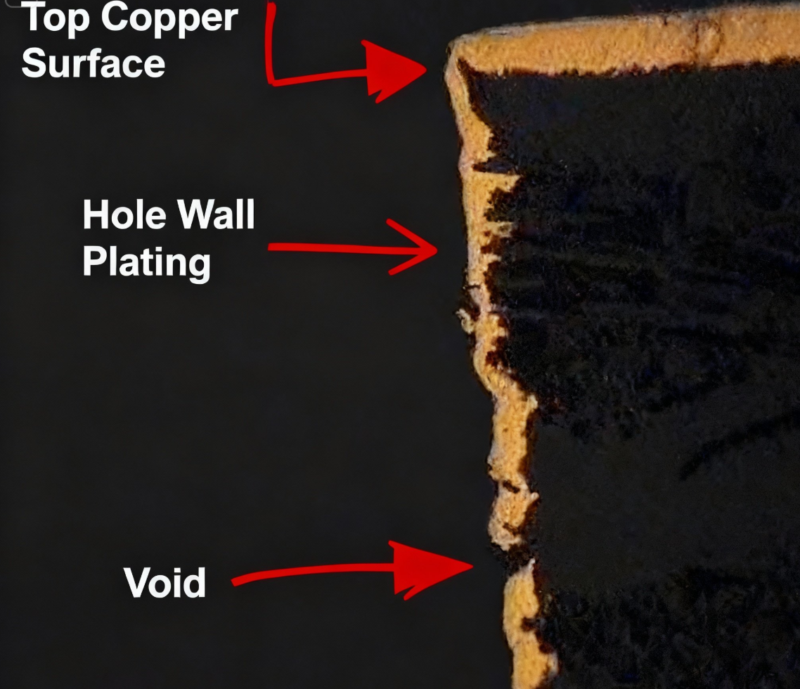
Plated Through-Hole Voids
Plated through-hole voids are sections within the PTH where the copper plating is either absent or incomplete. These voids frequently originate during the electroplating process due to factors like trapped air bubbles, contaminants, or uneven current distribution, all of which hinder uniform copper deposition.
Causes typically involve contamination within the plating bath (e.g., dust or organic residues), high aspect ratios (the ratio of hole depth to diameter, such as 10:1) making it challenging for the plating solution to reach the hole's center, and inadequate cleaning of drilled holes prior to plating, leaving debris that obstructs copper adhesion. Voids diminish the conductive area, increasing electrical resistance and potentially causing localized overheating or signal degradation. In severe instances, they can lead to open circuits.
Inner Layer Connection Failures
Inner layer connection issues arise when the copper plating within the PTH fails to establish proper electrical contact with the internal copper layers of a multilayer PCB. This defect often results in poor electrical conductivity between layers, thereby disrupting intended signal paths.
Causes include misalignment during drilling, preventing accurate intersection of the hole with inner layer copper, insufficient etching or cleaning processes leaving behind oxide layers that impede copper-to-copper bonding, and delamination of inner layers due to excessive heat or pressure during lamination, creating gaps. These issues can cause intermittent connections or complete signal loss, especially in intricate designs with a high number of layers.
Varied PTH Plating Thickness
The thickness of PTH plating should ideally be uniform, with a minimum of 20 micrometers as per industry standards like IPC-6012. However, variations in thickness can occur, with some areas being as thin as 10 micrometers or less, severely compromising the board's reliability.
Causes are often attributed to uneven current distribution during electroplating, frequently due to inadequate bath agitation, high aspect ratio holes where the plating solution struggles to penetrate evenly, and insufficient plating times, leading to an overall reduced copper deposit. Thin plating diminishes mechanical strength, making the PTH susceptible to cracking under stress. It also increases electrical resistance, negatively impacting signal integrity in high-speed circuits.
Step-by-Step Solutions for Troubleshooting PTH Defects
Having identified the common defects, let's now outline practical troubleshooting steps to diagnose and resolve these issues effectively. These solutions are designed to help pinpoint problems across the design, manufacturing, and post-production stages.
Diagnosing PTH Barrel Cracks
Step 1: Visual and Microscopic Examination
Employ a high-magnification microscope (at least 50x) to meticulously inspect the PTH barrel for any visible cracks. Cross-sectioning a sample board can reveal internal fractures that are not apparent from the surface.
Step 2: Thermal Stress Testing
Subject the PCB to thermal cycling tests (e.g., -40°C to 85°C for 100 cycles) to simulate real-world operational stresses. During these tests, continuously monitor for any changes in electrical continuity using a multimeter to detect the progression of cracks.
Solutions: Optimize drilling parameters to achieve smoother hole walls, thereby reducing stress concentration points. Select PCB materials with a lower CTE (e.g., below 15 ppm/°C) to minimize the impact of thermal expansion mismatch. Increase the copper plating thickness to at least 25 micrometers for enhanced mechanical durability.
Addressing Plated Through-Hole Voids
Step 1: X-Ray Inspection
Utilize X-ray imaging technology to non-destructively detect internal voids within the PTH plating. This method is particularly effective for boards with high component density.
Step 2: Process Review
Carefully review the electroplating process logs for any anomalies in current density (ideally maintained between 15-25 ASF, or amperes per square foot) or variations in the plating bath's chemical composition.
Solutions: Implement rigorous cleaning procedures post-drilling, such as ultrasonic cleaning, to ensure all debris is removed from the holes. Adjust plating bath agitation to ensure a uniform flow of the plating solution, especially crucial for high aspect ratio holes. In the design phase, limit hole aspect ratios to 6:1 or less to improve plating consistency.
Resolving Inner Layer Connection Issues
Step 1: Continuity Testing
Employ a netlist-based tester to meticulously check the electrical connectivity between PTHs and inner layers. A resistance reading exceeding 10 milliohms may strongly suggest a compromised connection.
Step 2: Cross-Section Analysis
Perform a destructive cross-section of a sample board to visually inspect the PTH alignment with inner layers under a microscope. Look for any visible gaps or evidence of oxide buildup at the critical connection points.
Solutions: Enhance drilling accuracy by utilizing advanced CNC machines, aiming for a tolerance of ±0.002 inches. Apply a desmear process after drilling to effectively remove any resin smears and improve copper adhesion to the inner layers. Carefully control lamination temperatures (e.g., keeping them below 180°C for standard FR-4 materials) to prevent delamination.
Ensuring Consistent PTH Plating Thickness
Step 1: Thickness Measurement
Employ microsectioning techniques or eddy current testing to accurately measure the copper thickness at multiple points along the PTH barrel. The goal is a minimum of 20 micrometers, in accordance with IPC standards.
Step 2: Plating Process Audit
Review the plating time and current settings in detail. A plating duration of 60-90 minutes at 20 ASF is typically sufficient for standard PTHs.
Solutions: Extend the plating duration if the measured thickness falls below specification, while diligently monitoring for potential risks of over-plating. Consider implementing pulse plating techniques to achieve better copper distribution in high aspect ratio holes. Regularly maintain and filter plating baths to prevent contamination that could adversely affect deposition uniformity.
Effective PTH Repair Methods for Damaged Holes
Despite meticulous efforts, PTHs can occasionally sustain damage during manufacturing or assembly. In such scenarios, repairing these holes is often a more economical choice than discarding the entire board. Here are established PTH repair methods to restore functionality.
Utilizing Eyelets or Funnelets
Eyelets or funnelets are small metallic inserts specifically designed to reinforce or repair compromised PTHs. They are pressed into the hole to establish a new, reliable conductive pathway.
Process: Clean the damaged PTH meticulously to remove any debris or residual plating. Select an eyelet with a diameter that precisely matches the existing hole. Insert and crimp the eyelet using a specialized tool to ensure a secure and stable fit. Finally, solder the eyelet to guarantee robust electrical connectivity.
Best For: Boards with isolated PTH damage where a comprehensive re-plating procedure is not practical.
Re-Plating Damaged Holes
For boards exhibiting multiple damaged PTHs, a re-plating process can be a viable and effective solution. This involves carefully stripping the old copper layer and subsequently applying a new one.
Process: Strip the existing copper using a suitable chemical etchant, ensuring no residue remains. If necessary, re-drill the holes to restore their precise dimensions. Re-plate the holes using an electroplating setup, aiming for a copper thickness of 25 micrometers.
Best For: High-value boards where maintaining the original design integrity and performance is paramount.
Proactive Strategies for Preventing Future PTH Defects
Prevention is always superior to repair. Integrating these best practices into your PCB design and manufacturing workflows will significantly minimize the occurrence of PTH defects.
Design and Material Considerations
In the design phase, strive to keep hole aspect ratios below 6:1 and consciously avoid placing PTHs in areas prone to high mechanical stress, such as near board edges. When selecting materials, opt for substrates with stable thermal properties (e.g., a CTE of 12-15 ppm/°C) to mitigate stress during temperature fluctuations.
Process Control and Testing
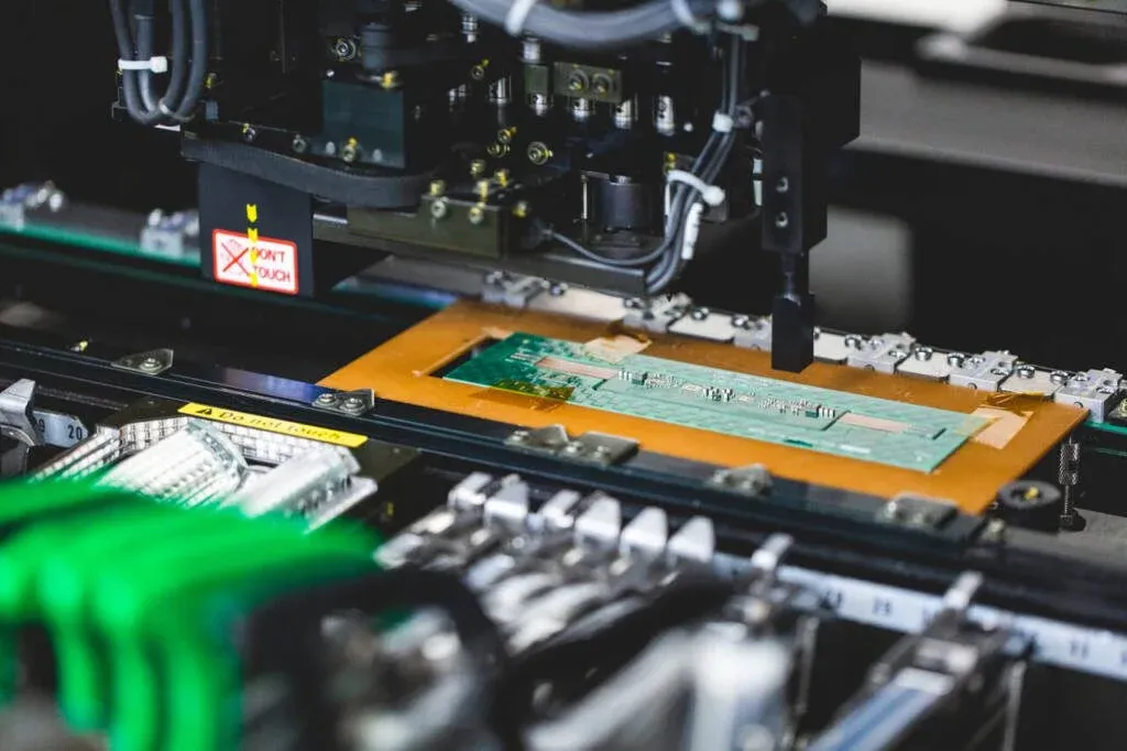
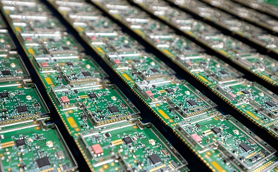
Implement rigorous quality checks throughout the drilling, plating, and lamination stages of manufacturing to identify and rectify issues early. Utilize advanced testing methods, such as Automated Optical Inspection (AOI) and X-ray systems, to detect defects before the assembly process begins.
Conclusion: Achieving Flawless PCB Production
Effectively troubleshooting common plated through-hole defects—including barrel cracks, voids, inner layer connection problems, and inconsistent plating thickness—does not have to be an overwhelming challenge. By thoroughly understanding their root causes, employing systematic diagnostic techniques, and applying appropriate PTH repair methods, you can ensure the unwavering reliability and consistent performance of your PCBs. Furthermore, a proactive approach emphasizing thoughtful design and stringent manufacturing controls will substantially reduce the likelihood of these issues, resulting in long-term savings in both time and cost.
At AIVON, as a well-known and large PCB manufacturer, we are dedicated to providing engineers with the essential tools and knowledge required to achieve impeccable PCB production. Whether you are tackling an intricate multilayer design or a straightforward prototype, addressing PTH defects with precision is a cornerstone of success. Keep this guide readily accessible for your upcoming projects, and witness a marked improvement in your board quality.