Introduction
High-voltage printed circuit boards demand precise control over trace dimensions to ensure reliable operation under demanding electrical conditions. Engineers designing these boards must balance trace width for adequate current handling with sufficient spacing to prevent dielectric breakdown and arcing. Improper sizing leads to overheating, insulation failure, or catastrophic shorts, compromising system integrity. This article explores the interplay between trace width calculations and spacing requirements, drawing on established industry standards for guidance. By mastering these elements, designers can optimize PCB performance for applications like power supplies, inverters, and industrial controls. Understanding these principles enables electric engineers to create robust, compliant designs from the outset.
Why Trace Width and Spacing Matter in High-Voltage PCBs
Trace width primarily determines a conductor's ability to carry current without excessive temperature rise, which is critical in high-voltage circuits where power levels often demand high currents. Narrow traces increase resistance, leading to I squared R losses that generate heat and degrade nearby insulation. Conversely, spacing between traces governs voltage isolation, preventing flashover across air gaps or along board surfaces. In high-voltage environments, insufficient PCB trace spacing high voltage invites partial discharges or creepage failures, especially under humidity or contamination. These factors directly impact reliability, safety certifications, and long-term field performance. Adhering to standards like IPC-2221 ensures designs withstand operational stresses without unexpected failures.
High-voltage PCBs operate where voltages exceed typical low-power boards, amplifying risks from minor dimensional errors. For instance, high current trace width must accommodate peak loads while spacing accounts for transient spikes. Neglecting these can result in reduced mean time between failures or non-compliance with safety norms. Engineers prioritize these during layout to avoid costly respins. Proper mastery supports compact designs without sacrificing margins. Ultimately, informed decisions here elevate PCB quality and accelerate time to market.
Technical Principles of Trace Width and Spacing
Current-Carrying Capacity and Trace Width Fundamentals
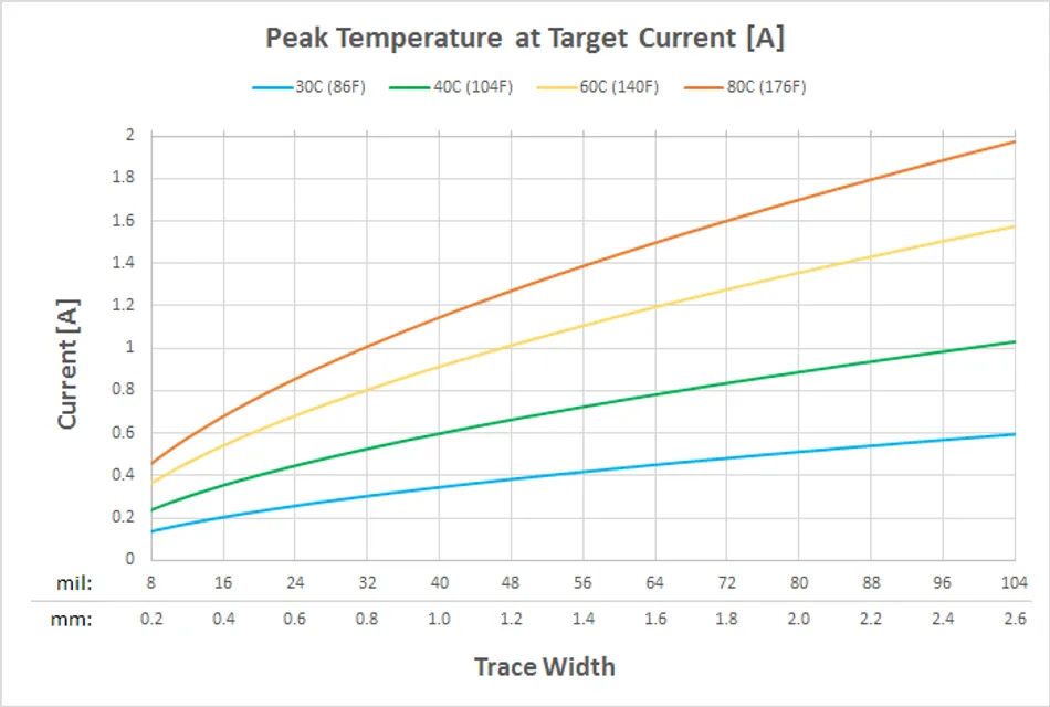
Trace width calculation hinges on the relationship between current, cross-sectional area, and allowable temperature rise. Wider traces offer larger copper cross-sections, reducing resistance and heat generation per the power dissipation formula P equals I squared R. Standards provide charts relating current to width for given copper thicknesses and layer positions, external traces dissipating heat better than internal ones due to convection. Factors like board thickness, adjacent planes, and ambient conditions influence thermal performance. IPC-2152 outlines methodologies using graphical data from extensive testing, accounting for variables such as vacuum versus air environments. This structured approach allows precise high voltage trace width calculation tailored to specific designs.
Temperature rise remains a key constraint, typically limited to avoid delamination or solder joint stress. Heat transfers via conduction to the board, convection to air, and radiation, with wider traces enhancing dissipation. Internal layers rely more on conduction through dielectrics, often requiring broader widths than external counterparts. Copper weight, from 1 oz to heavier foils, directly scales capacity. Designers adjust for these in simulations or nomographs from the standard. Consistent application prevents hotspots that accelerate aging in high-voltage applications.
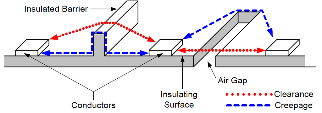
Voltage Isolation: Clearance and Creepage Distances
Clearance defines the shortest air path between conductors, resisting dielectric breakdown under peak voltages. Creepage measures surface path length, vulnerable to tracking from contamination or moisture. Both scale with operating voltage, pollution degree, material comparative tracking index, and coatings. IPC-2221 specifies minimums via tables categorized by conductor location, such as internal versus external uncoated or coated. For higher voltages, increments apply per additional volt beyond baselines. These ensure electric field strengths stay below breakdown thresholds.
Pollution degree one assumes clean environments, while degree three demands wider spacings for conductive contaminants. Material groups based on CTI dictate creepage tolerances, higher values permitting tighter layouts. Altitude adjustments increase clearances due to reduced air density, and conformal coatings can relax requirements. Trace spacing for high voltage thus demands holistic consideration of assembly and end-use conditions. Engineers classify nets accordingly to enforce rules in design software. This layered principle upholds insulation integrity across lifecycles.
Practical Solutions and Best Practices
Calculating Trace Width for High-Current High-Voltage Traces
Begin high voltage trace width calculation by identifying peak current, allowable temperature rise, and copper specifications. Consult IPC-2152 charts for unadjusted cross-sectional area based on current and rise relative to local board temperature. Apply multipliers for copper thickness, external or internal placement, board material, thickness, and nearby planes. Divide the adjusted area by thickness to yield width. Verify with thermal simulations incorporating vias and power planes for accuracy. This iterative process optimizes without excess material use.
For high current trace width, prioritize external layers where possible for superior cooling. Parallel traces or pours boost effective capacity, treated as wider equivalents. Account for derating in dense layouts or high ambients. Standard copper weights suffice for most, but heavier foils suit extreme demands. Document assumptions for fab handover. Regular validation against prototypes confirms predictions.
Implementing PCB Trace Spacing for High Voltage
Select the appropriate IPC-2221 table based on voltage type, peak or RMS, and environmental factors. Determine pollution degree and CTI group from material datasheets. Look up minimum clearance or creepage, adding altitude corrections if above sea level. Define net classes in CAD with custom rules overriding defaults. Use slots or barriers to extend effective creepage without enlarging boards. Conformal coatings post-assembly can enable tighter initial spacings.
Incorporate guard traces or grounded planes to shield sensitive areas. Route high-voltage nets away from edges and connectors prone to contamination. Verify spacing in 3D views, checking vias and pads. Manufacturing tolerances necessitate design margins. Post-etch inspections confirm compliance. These practices minimize arcing risks systematically.
Integrated Design Strategies
Combine width and spacing rules early in schematic capture via net assignments. High-power HV traces benefit from wider profiles reducing voltage drops, but demand proportional spacings per the 3W rule where separation exceeds three times width. Layer stacking isolates HV sections. Vias thermal reliefs aid current flow without hotspots. DFMs review ensures fab capabilities align. Simulation tools model fields and thermals pre-layout.
Troubleshooting Common High-Voltage PCB Issues
Overheating signals undersized traces; measure resistance and monitor temps under load. Arcing manifests as carbon tracks; inspect for spacing violations or contamination. Simulations reveal hotspots before fab. Prototype testing under accelerated conditions validates. Adjust iteratively per standard charts. Field failures trace back to overlooked factors like humidity.
Conclusion
Mastering trace width and spacing unlocks reliable high-voltage PCB designs. Current capacity per IPC-2152 ensures thermal stability, while IPC-2221 spacings safeguard isolation. Practical calculations, informed by environmental realities, yield optimized layouts. Engineers applying these structured methods enhance performance and compliance. Prioritize standards integration for enduring results. Future designs will leverage evolving simulations alongside these foundations.
FAQs
Q1: How do you perform high voltage trace width calculation?
A1: High voltage trace width calculation starts with peak current and temperature rise limits from IPC-2152 charts. Determine cross-sectional area, apply multipliers for layers, copper weight, and planes, then compute width. External traces handle more current due to better cooling. Verify thermally to avoid hotspots in power applications. This ensures safe operation without excess size.
Q2: What factors influence PCB trace spacing high voltage?
A2: PCB trace spacing high voltage depends on peak voltage, pollution degree, CTI material group, and coatings per IPC-2221 tables. Clearance governs air paths and creepage governs surface paths, with increments for altitude. Select categories like uncoated external or coated, and use net classes to automate rule enforcement. Include margins to cover tolerances for reliability.
Q3: Why is high current trace width critical in HV designs?
A3: High current trace width prevents excessive heating that weakens insulation in HV boards. Wider traces lower resistance, aiding dissipation via convection and conduction. IPC-2152 guides sizing considering local temperatures and planes. Undersizing risks delamination or failures. Balance trace width with required spacing for holistic integrity.
Q4: How does trace spacing for high voltage affect layout?
A4: Trace spacing for high voltage dictates routing freedom, requiring wider gaps at higher voltages per standards. Use guard traces and layer isolation to manage fields. Conformal coatings can relax rules post-fab. 3D checks confirm compliance around pads and vias. Early planning enables compact yet safe designs.
References
IPC-2221B — Generic Standard on Printed Board Design. IPC, 2012
IPC-2152 — Standard for Determining Current Carrying Capacity in Printed Board Design. IPC, 2009