Introduction
In high-speed digital PCB design, the layer stackup serves as the foundation for achieving reliable performance. Engineers face increasing challenges from faster signal rise times and higher data rates, which amplify issues like signal distortion and electromagnetic interference. Proper PCB stackup design directly influences signal integrity by controlling impedance and providing low-inductance return paths. It also plays a critical role in EMI reduction PCB strategies through effective shielding and plane arrangements. This article explores structured approaches to high-speed PCB layer stack configuration, focusing on practical engineering principles for electric engineers.
Understanding PCB Stackup in High-Speed Designs
A PCB stackup refers to the specific arrangement of copper layers, dielectrics, and planes in a multilayer board. In high-speed applications, this configuration determines transmission line characteristics and field containment. Multilayer PCB stackup becomes essential as designs exceed gigabit speeds, where microstrip and stripline geometries dominate. Poor stackup leads to uncontrolled impedance variations, increasing reflections and timing skew. Conversely, optimized setups ensure consistent electrical performance across frequencies.
The relevance stems from modern protocols demanding low bit error rates. Engineers must balance mechanical stability with electrical needs during the initial layout phase. IPC-2221 provides foundational guidelines for such designs, emphasizing layer sequencing for integrity.
Key Principles of Signal Integrity in PCB Stackup Design
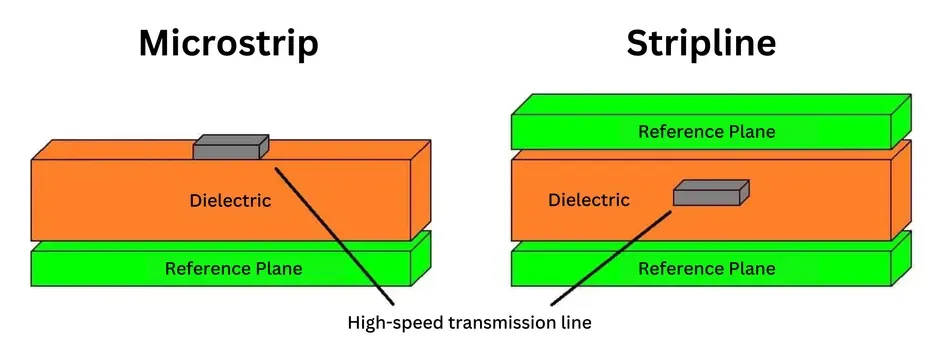
Signal integrity relies on maintaining characteristic impedance through controlled dielectric spacing and reference planes. High-speed signals propagate as guided waves, confined by adjacent ground or power planes. In stripline configurations, signals between planes experience symmetric fields, reducing radiation. Microstrip lines on outer layers couple more to free space, heightening EMI risks. Return currents follow the path of least impedance, typically mirroring signals on reference planes.
Crosstalk arises from mutual inductance and capacitance between adjacent traces. Closer spacing amplifies capacitive coupling, while parallel runs induce inductive effects. PCB stackup design mitigates this by separating sensitive layers with planes. Plane capacitance between power and ground layers stabilizes voltage, filtering noise.
Impedance mismatches cause ringing and overshoot. Uniform dielectric thickness ensures predictable propagation delays. Engineers calculate effective dielectric constants based on material stacks.
Mechanisms of EMI and Crosstalk in High-Speed PCB Layer Stack
EMI originates from unintended radiation of switching currents forming loop antennas. Large current loops on outer layers radiate efficiently, coupling to nearby circuits. Ground planes act as shields by providing low-impedance return paths and image currents. In EMI reduction PCB approaches, adjacent signal-ground pairs contain fields within the board.
Crosstalk control PCB techniques focus on minimizing coupling coefficients. Forward crosstalk dominates at high frequencies due to near-end and far-end effects. Buried signal layers flanked by planes exhibit lower coupling than surface routes. Power plane ground plane stackup pairing creates distributed capacitance, decoupling noise.
Asymmetric stacks induce warpage from thermal expansion mismatches. Balanced configurations maintain flatness during reflow. IPC-6012 outlines performance specs ensuring stack integrity under stress.
Strategies for Optimizing Multilayer PCB Stackup
Ground-Referenced Signal Layers
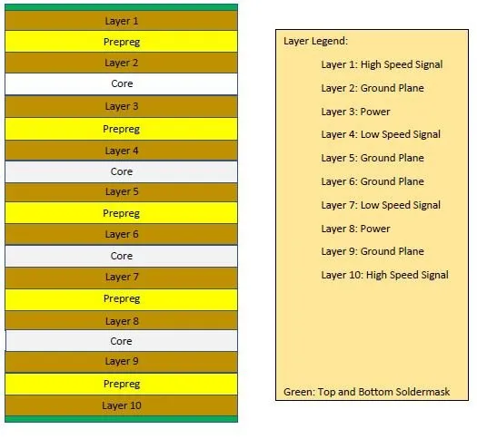
Position high-speed signals adjacent to continuous ground planes for best integrity. This setup provides image return paths directly beneath traces, minimizing loop area. In a 6-layer high-speed PCB layer stack, layers 2 and 5 serve as signals between L1-ground and power-L6 ground. Thinner dielectrics near signals tighten impedance control.
Power planes should couple closely to ground for decoupling. Split planes require stitching vias to avoid slots interrupting returns. Avoid routing signals over plane splits.
Power Plane and Ground Plane Stackup Configurations
Pair power and ground planes adjacently to form a capacitor reservoir. This reduces inductance in power distribution networks. In multilayer PCB stackup, alternate signal-ground-power sequences. Wide power planes distribute current evenly, preventing voltage droop.
Ground planes unify returns, preventing noise propagation. Multiple ground planes segment domains for analog-digital separation. Decoupling capacitors bridge planes at IC pins.
Crosstalk Control and EMI Reduction Techniques
Separate high-speed layers by at least one plane to attenuate coupling. Orthogonal routing on adjacent signals reduces broadside capacitance. Guard traces with grounds further isolate. For EMI reduction PCB, outer layers suit low-speed nets, burying clocks internally.
Via fences along edges shield board radiation. Controlled impedance targets, like 50 ohms single-ended, demand precise stack planning. Simulations verify pre-layout choices.
Best Practices for High-Speed PCB Stackup Design
Symmetrize the stack around the core for mechanical stability. Equal prepreg buildup on both sides prevents bowing. Use low-loss dielectrics for frequencies above 1 GHz. Material selection aligns CTE for reliability.
Document stack details including foil weights and resin percentages. Collaborate with fabricators early for manufacturability. Iterate via field solver tools for impedance profiles.
In dense designs, dedicate inner layers to high-speed nets. Surface layers handle components and slower signals. Stitch ground vias densely near signals.
Troubleshooting Common Stackup Issues
Excessive crosstalk signals poor layer separation. Measure TDR for impedance steps correlating to dielectric variations. EMI failures often trace to inadequate shielding; probe radiated fields. Adjust by adding planes or rerouting.
Warpage from asymmetric stacks fails assembly. Balance thicknesses per IPC guidelines. Signal skew from unequal lengths requires length matching.
Power noise indicates insufficient plane capacitance. Add local decouplers.
Conclusion
Effective PCB stackup design integrates signal integrity, crosstalk control, and EMI minimization into a cohesive structure. Ground-referenced signals, paired planes, and symmetric builds form core strategies. Electric engineers benefit from principled layer assignments tailored to speed and density. Adhering to standards ensures robust high-speed performance. Prioritize stackup early to avoid costly respins.
FAQs
Q1: What is the role of ground planes in high-speed PCB layer stack for EMI reduction PCB?
A1: Ground planes provide low-impedance return paths and shield signals from radiating. Placing them adjacent to signal layers confines electric fields, reducing EMI. This power plane ground plane stackup also decouples power noise. Proper stitching prevents slots that leak emissions.
Q2: How does PCB stackup design control crosstalk in multilayer boards?
A2: Separate signal layers with reference planes to minimize mutual coupling. Orthogonal orientations on adjacent layers reduce broadside capacitance. Buried routing in striplines offers superior isolation over microstrips. Simulations predict coupling levels pre-layout.
Q3: Why choose stripline over microstrip in high-speed PCB layer stack?
A3: Striplines embed signals between planes for symmetric fields and lower radiation. They maintain tighter impedance control with thinner dielectrics. Microstrips suit lower speeds but expose fields, increasing EMI risks. Optimal for gigabit signals.
Q4: What are key considerations for power plane ground plane stackup in crosstalk control PCB?
A4: Close coupling forms capacitance for noise filtering. Avoid splits under signals to preserve returns. Multiple grounds segment noisy domains. This enhances integrity in dense multilayer PCB stackup.
References
IPC-2221C — Generic Standard on Printed Board Design. IPC, 2023
IPC-6012F — Qualification and Performance Specification for Rigid Printed Boards. IPC, 2023


