Introduction
In the realm of medical electronics, where space constraints and reliability demands converge, stacked via PCBs play a pivotal role in enabling compact, high-performance designs. These structures, integral to high density interconnect (HDI) technology, allow for vertical interconnections across multiple layers in printed circuit boards tailored for medical applications. As medical devices evolve toward miniaturization, such as in implantable pacemakers, portable diagnostics, and advanced imaging systems, the use of stacked via PCB in medical devices becomes essential for achieving superior signal integrity and power distribution. Electrical engineers must prioritize medical device PCB design that balances density with unwavering safety, adhering to rigorous industry benchmarks to prevent failures that could compromise patient outcomes. High-performance medical PCBs incorporating stacked vias not only optimize routing efficiency but also ensure compliance with essential safety protocols in PCB for medical applications.
What Are Stacked Via PCBs and Why Do They Matter in Medical Devices?
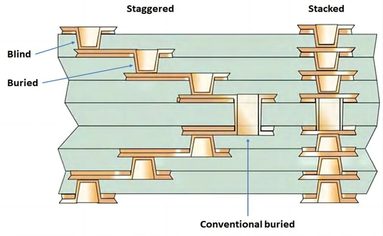
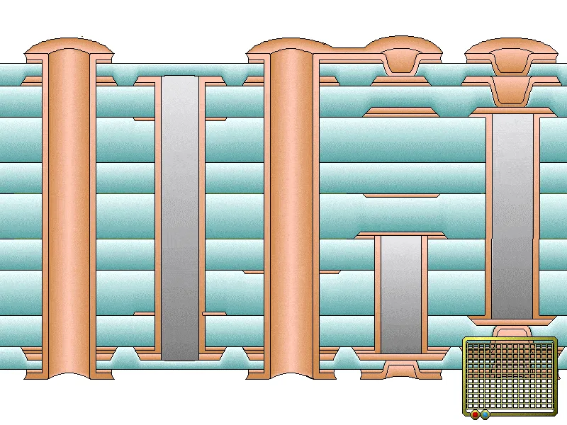
Stacked via PCBs feature multiple microvias aligned vertically, one directly atop another, to bridge non-adjacent layers in multilayer boards. This configuration contrasts with staggered vias, where offsets provide separation, and proves vital in HDI constructions common to medical electronics. In medical device PCB design, stacked vias facilitate the dense integration required for fine-pitch components like BGAs in devices handling real-time data processing or sensor arrays. Their relevance stems from the need for high-performance medical PCBs that maintain electrical continuity under operational stresses, including thermal cycling and mechanical vibration inherent to body-worn or implantable systems. Without such interconnects, achieving the necessary layer density for PCB for medical applications would demand thicker boards, increasing size and weight, which directly conflicts with clinical usability. Engineers value stacked via PCB in medical devices for enabling shorter signal paths that reduce latency and electromagnetic interference, critical factors in life-sustaining equipment.
Technical Principles of Stacked Vias in High-Density Medical PCBs
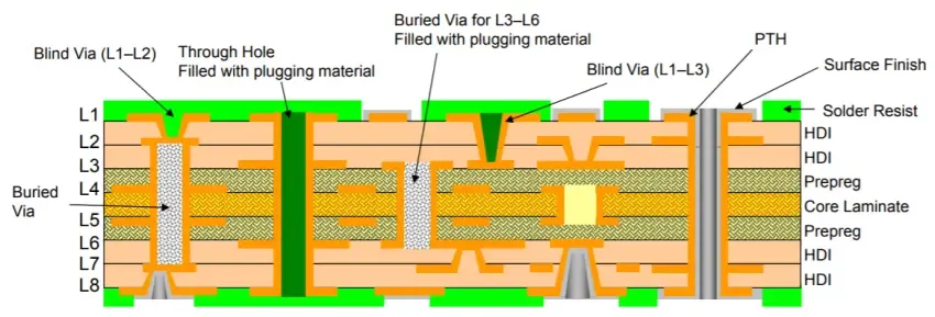
The formation of stacked vias begins with laser drilling of microvias into dielectric layers, followed by sequential lamination to build up the structure. Each via level undergoes electroless copper deposition, electroplating, and often conductive filling to ensure planar surfaces for subsequent layers. Aspect ratios, defined as depth to diameter, must remain low, ideally below 0.8 to 1, promoting uniform plating and mitigating void formation during fabrication. In medical electronics, coefficient of thermal expansion (CTE) mismatches between copper and dielectrics exacerbate stresses during reflow or operation, potentially leading to barrel or corner cracking in stacked configurations spanning three or more levels. Proper material selection, favoring laser-drillable resins with homogeneous glass reinforcement, enhances adhesion and reduces z-axis expansion disparities. These principles underpin the reliability of stacked via PCB in medical devices, where even minor discontinuities can propagate signal degradation over time.
Understanding failure mechanisms is crucial: thermal excursions beyond the glass transition temperature induce differential expansion, compressing via walls in stacked arrays. IPC-2226 outlines stack-up types like 2+N+2, where outer microvia layers connect to an inner core, optimizing for density while distributing stress. Electrical engineers simulate these effects early to predict impedance discontinuities, ensuring high-performance medical PCBs sustain multi-gigahertz signals without excessive insertion loss. Sequential processes demand precise registration, as misalignment compounds across levels, amplifying risks in compact medical designs.
Design Best Practices for Stacked Vias in Medical Device PCB Design
Engineers should limit stacked vias to two levels where possible, favoring staggered offsets for deeper connections to alleviate cumulative stress. Copper filling or capping vias per established guidelines prevents solder wicking and bolsters mechanical integrity during assembly. Optimal pad sizing, with capture pads at least 80% larger than via diameter, secures plating adhesion, while maintaining clearances three times the via diameter from adjacent traces curbs crosstalk. In PCB for medical applications, stack-ups must accommodate IPC Class 3 criteria, demanding flawless annular rings and full barrel fill to withstand environmental rigors. Collaborating on drill files early verifies manufacturability, specifying parameters like 4 to 6 mil diameters for microvias to balance precision and current capacity. These practices elevate medical device PCB design, yielding boards resilient to the vibrations and sterilizations encountered in clinical settings.
Signal integrity demands placing high-speed traces on adjacent layers to minimize stub lengths, supplemented by ground vias for return paths. Power vias benefit from larger drills to dissipate heat, avoiding hotspots in densely packed medical electronics. Pre-layout verification against IPC-2226 ensures compliance, while D-coupon inclusion monitors via chain resistance in simulations.
Manufacturing Processes and Quality Assurance for High-Performance Medical PCBs
Fabrication commences with core lamination, followed by laser ablation for blind vias, plasma cleaning, and copper seeding. Stacked structures require iterative cycles: drilling, desmear, plating, filling, and planarization via chemical mechanical polishing to achieve flatness for imaging. Conductive epoxy or electroplated copper fills mitigate voids, essential for stacked via reliability under shear forces. In medical applications, processes align with IPC Class 3, verifying plating thicknesses exceed 20 microns without cracks via cross-section analysis. Automated optical inspection precedes flying probe testing, confirming continuity across via chains before final lamination.
Quality assurance extends to interconnect stress testing (IST), applying thermal and electrical loads to detect latent defects like microcracks. Thermal cycling from -55°C to 125°C simulates operational extremes, with resistance shifts under 5% indicating robustness. X-ray and microsectioning reveal fill quality, ensuring no delamination threatens PCB for medical applications.
Challenges and Mitigation Strategies in Stacked Via PCB Reliability
Stacked vias heighten risks from CTE-induced cracking, particularly beyond two levels, as stresses accumulate vertically. Mitigation involves homogeneous stack-ups with matched materials and minimal lamination cycles to preserve dielectric integrity. In high-performance medical PCBs, staggered alternatives offset centers by more than via diameter, distributing loads and enhancing cycle life. IEC 60601-1 mandates essential performance under fault conditions, compelling designs that avert single-point failures in critical paths. Engineers employ failure mode analysis to prioritize via placement away from bend radii in flex-rigid hybrids common to wearables.
Practical troubleshooting includes back-drilling unused stubs for RF paths and tenting vias to shield against contaminants. Post-assembly bake-out removes moisture, preventing popcorning in stacked structures during subsequent reflows.
Conclusion
Stacked via PCBs empower medical device PCB design by delivering the density and efficiency demanded by modern medical electronics, while rigorous adherence to principles like low aspect ratios and copper filling safeguards performance. Balancing compactness with IPC Class 3 reliability and IEC 60601-1 safety ensures these high-performance medical PCBs excel in demanding environments. Electrical engineers, by integrating best practices from stack-up optimization to IST validation, mitigate risks inherent to stacked configurations. Ultimately, thoughtful implementation of stacked via PCB in medical devices upholds patient safety, driving innovation in PCB for medical applications without compromise.
FAQs
Q1: What role do stacked vias play in medical device PCB design?
A1: Stacked vias enable vertical interconnections in HDI PCBs, crucial for dense routing in compact medical electronics like implants and diagnostics. They support fine-pitch components by connecting multiple layers efficiently, reducing board size while preserving signal integrity. Following IPC-2226 guidelines limits stacking to two levels for reliability, ensuring high-performance medical PCBs meet safety thresholds in PCB for medical applications. Proper design prevents thermal stress failures common in medical environments.
Q2: Why prefer staggered over stacked vias in high-performance medical PCBs?
A2: Staggered vias offset positions across layers, distributing mechanical stress better than direct stacking, which risks cracking under thermal cycling. This configuration suits deeper layer connections in medical device PCB design, enhancing cycle life without added complexity. In PCB for medical applications, staggered structures minimize impedance discontinuities for high-speed signals, aligning with IPC Class 3 demands. Engineers select them for superior reliability in stacked via PCB in medical devices.
Q3: How does IEC 60601-1 influence stacked via PCB in medical devices?
A3: IEC 60601-1 establishes safety and performance criteria for medical electrical equipment, requiring PCBs to endure fault conditions without hazardous outputs. For stacked via designs, it necessitates robust interconnects resistant to environmental stresses, verified through testing like thermal shock. This ensures high-performance medical PCBs in medical electronics maintain essential functions, guiding material and process choices in medical device PCB design.
Q4: What testing ensures reliability of stacked vias in PCB for medical applications?
A4: Interconnect stress testing (IST) monitors via resistance under combined thermal and electrical loads, detecting microcracks early. Thermal cycling and reflow simulations per IPC methods confirm endurance, with shifts below 5% acceptable. Cross-section analysis verifies plating and fill quality, vital for high-performance medical PCBs. These protocols safeguard stacked via PCB in medical devices against field failures.
References
IPC-2226 — Design Standard for High Density Interconnect (HDI) Printed Boards. IPC
IPC-6012E — Qualification and Performance Specification for Rigid Printed Boards. IPC, 2015
IEC 60601-1 — Medical Electrical Equipment: General Requirements for Basic Safety and Essential Performance. IEC
IPC-A-600K — Acceptability of Printed Boards. IPC, 2020


