Introduction
In high-density interconnect (HDI) printed circuit boards, vias serve as critical interconnects between layers, enabling compact designs for modern electronics. Engineers often face the choice between stacked vias and staggered vias when optimizing for density, reliability, and manufacturability. This stacked vs staggered via comparison directly impacts signal integrity, board space utilization, and long-term performance under thermal stress. Understanding the trade-offs helps in selecting the appropriate configuration for specific project requirements. As PCB complexity increases with finer pitch components, the decision influences overall design success.
What Are Stacked Vias and Staggered Vias?
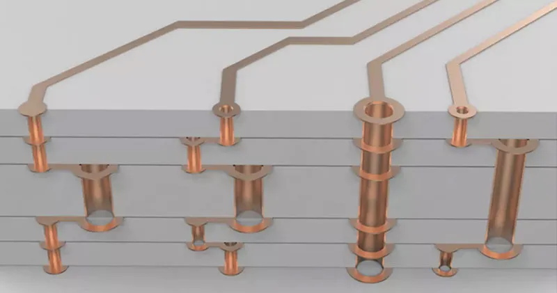
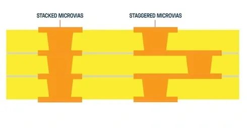
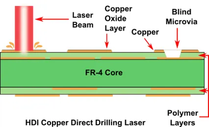
Stacked vias consist of multiple blind or microvias aligned directly on top of each other along the same vertical axis, forming a continuous column through several layers. This configuration connects non-adjacent layers efficiently without penetrating the entire board thickness. Staggered vias, by contrast, feature microvias positioned with intentional offsets on adjacent layers, landing on small pads or traces that fan out slightly before reconnecting. Each via in a staggered structure has its own drill axis, avoiding direct superposition.
These via types matter in HDI PCBs where through-hole vias would consume excessive space and introduce parasitic effects. Stacked vias excel in ultra-compact applications, while staggered vias prioritize mechanical robustness. The choice aligns with project constraints like layer count, component density, and environmental exposure. Proper selection prevents issues such as delamination or signal degradation during operation.
Technical Principles of Stacked and Staggered Vias
The fundamental mechanism of stacked vias relies on sequential lamination and precise laser drilling to create aligned openings, followed by electroplated copper filling for structural integrity and conductivity. Copper filling eliminates voids that could lead to stress concentrations, ensuring a solid interconnect path. However, the direct stacking amplifies coefficient of thermal expansion (CTE) mismatches between copper and dielectric materials during temperature excursions. This induces shear stresses at via interfaces, particularly beyond two stacked layers.
Staggered vias distribute these stresses by offsetting via positions, allowing each microvia to interface with a larger landing pad on intermediate layers. Manufacturing involves fewer critical alignment steps, as vias do not share axes, reducing registration errors. Laser ablation removes dielectric precisely, and plating occurs without full filling for internal vias. The offset design mitigates barrel cracking by spreading mechanical loads across a wider area.
Aspect ratio, defined as via depth to diameter, plays a key role in both configurations, with industry guidelines recommending ratios near 1:1 for optimal plating and reliability. IPC standards emphasize controlled aspect ratios to minimize plating defects and enhance thermal cycle endurance. Electrical performance differs too, as stacked vias offer shorter signal paths with lower inductance, while staggered vias may introduce minor discontinuities.
Stacked Via Advantages and Disadvantages
Stacked vias provide significant advantages in space-constrained designs by enabling vertical routing through multiple layers without expanding the board footprint. This compactness supports higher component densities, ideal for applications like smartphones or wearables. Signal integrity benefits from reduced stub lengths and uniform impedance profiles, minimizing reflections and electromagnetic interference. The filled structure also enhances current-carrying capacity and thermal dissipation.
Despite these benefits, stacked vias pose challenges in reliability due to concentrated stresses at stack interfaces. Thermal cycling exacerbates CTE-induced cracking, especially in multilayer stacks. Manufacturing complexity arises from additional process steps like planarization and void-free filling, demanding advanced equipment and quality controls.
Staggered Via Advantages and Disadvantages
Staggered vias shine in reliability by dispersing mechanical and thermal stresses across offset positions, reducing the risk of via wall detachment or fracturing. This makes them suitable for environments with vibration or repeated temperature swings, common in automotive or industrial electronics. Fabrication simplicity lowers defect rates, as offset placement tolerates minor drill misalignments better than precise stacking.
On the downside, staggered vias require more real estate on intermediate layers for landing pads and fanouts, potentially complicating routing in dense areas. Signal paths lengthen slightly, which could affect high-speed designs sensitive to inductance variations. However, crosstalk remains low due to separated axes.
Stacked Via Reliability vs Staggered Via
Reliability comparisons highlight staggered vias' superiority in enduring thermal-mechanical stresses, as offsets prevent stress hotspots that plague stacked configurations. In stacked vias, cumulative layer interactions amplify failures like corner cracking under CTE differential expansion. Staggered designs, by contrast, isolate each via's stress field, promoting even load distribution.
IPC-6012E outlines qualification tests for via performance, including thermal cycling, where staggered structures often demonstrate greater endurance. Copper filling in stacked vias bolsters strength but introduces void risks if plating is uneven. Engineers must simulate stress via finite element analysis to predict behaviors accurately.
Stacked Via Cost vs Staggered Via
Cost dynamics favor staggered vias due to streamlined manufacturing with fewer lamination cycles and no universal filling requirement. Stacked vias escalate expenses through specialized processes like electroplating fills and extra imaging steps. Sequential build-up for stacks demands tighter process controls, extending lead times.
Volume production amplifies these differences, as staggered vias scale more predictably without advanced tooling. Budget-conscious projects benefit from staggered approaches when space allows. Design tools aid cost estimation by modeling via counts and stack complexity.
Practical Best Practices for Via Selection
Begin with stack-up planning per IPC-2226 guidelines for HDI, assessing layer count and via transitions early. Prioritize staggered vias for three or more layer spans to enhance reliability, reserving stacks for density-critical zones. Maintain aspect ratios below 1:1, using larger diameters where possible to ease plating.
Collaborate with fabricators on capabilities, specifying fill types and offsets. Simulate thermal performance to validate choices, focusing on CTE-matched materials. For mixed configurations, transition gradually to balance density and robustness.
Quick stacked vs staggered via comparison:
- Space Usage: Stacked Vias — Minimal; Staggered Vias — Higher.
- Manufacturing Ease: Stacked Vias — Complex, multi-step; Staggered Vias — Simpler.
- Reliability: Stacked Vias — Stress-prone; Staggered Vias — Superior stress distribution.
- Signal Integrity: Stacked Vias — Excellent, short paths; Staggered Vias — Good, minor discontinuities.
- Cost: Stacked Vias — Higher; Staggered Vias — Lower.
Choosing the Right Via for Your Project
Evaluate project drivers: opt for stacked vias in ultra-dense, high-speed boards where space trumps longevity. Shift to staggered for reliable, cost-effective builds under harsh conditions. Hybrid use combines strengths, staggering outer stacks and stacking inner for optimization.
Conclusion
The stacked vs staggered via comparison reveals clear trade-offs in density, reliability, and economics. Stacked via advantages lie in compactness and signal performance, while staggered via advantages emphasize durability and affordability. Stacked via reliability vs staggered via favors the latter for thermal challenges, and stacked via cost vs staggered via underscores manufacturing impacts. Align choices with standards like IPC-6012E and project needs for optimal outcomes. Thoughtful selection ensures robust, efficient PCBs.
FAQs
Q1: What is the main difference in stacked vs staggered via comparison for HDI PCBs?
A1: Stacked vias align directly vertically for maximum density, while staggered vias offset positions to distribute stresses. This affects space, manufacturing, and endurance. Choose based on density needs versus reliability priorities in electric engineering designs. Stacked suits tight layouts; staggered excels in multi-layer reliability.
Q2: What are the stacked via advantages in high-density applications?
A2: Stacked via advantages include superior space efficiency and signal integrity from short, aligned paths. They reduce inductance and maintain impedance control effectively. Ideal for fine-pitch BGAs, though reliability demands careful filling and low aspect ratios.
Q3: Why do staggered via advantages include better reliability?
A3: Staggered via advantages stem from offset placement that spreads thermal-mechanical loads, minimizing cracking risks. They withstand cycling better than stacks by avoiding interface stress buildup. Cost savings arise from simpler processes, making them practical for industrial use.
Q4: In stacked via cost vs staggered via, which is more economical for prototypes?
A4: Staggered vias typically lower costs due to reduced complexity in drilling and plating. Stacked configurations add expenses from sequential steps and fills. For prototypes, staggered balances performance and budget unless density dictates otherwise.
References
IPC-6012E — Qualification and Performance Specification for Rigid Printed Boards. IPC, 2017
IPC-A-600K — Acceptability of Printed Boards. IPC, 2020
IPC-2226 — Sectional Design Standard for HDI Printed Boards. IPC, 2019