Introduction
Printed circuit board (PCB) designers often face critical decisions when selecting form factors, balancing functionality, fit, and budget constraints. Standard PCB sizes offer predictability and leverage established manufacturing efficiencies, making them a cornerstone for PCB cost optimization in high-volume projects. Custom PCB fabrication, on the other hand, provides flexibility for unique enclosures or space-limited applications but introduces variables that can escalate expenses. Understanding the trade-offs between these options is essential for electric engineers aiming to achieve PCB design for manufacturing principles while reducing PCB costs. This article explores the technical and practical aspects of standard versus custom form factors, drawing on industry-aligned insights to guide informed choices. By prioritizing form factor decisions early, teams can minimize waste, improve yield, and streamline production.

Defining Standard PCB Sizes and Custom PCB Fabrication
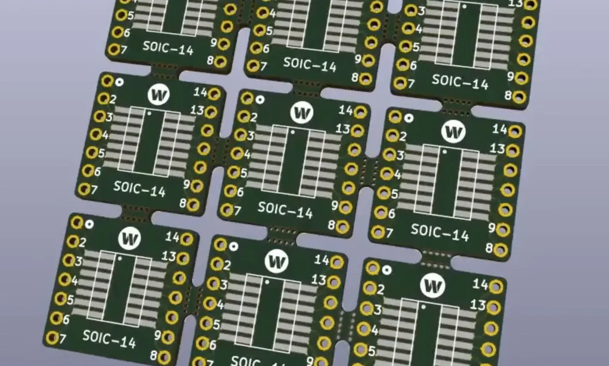
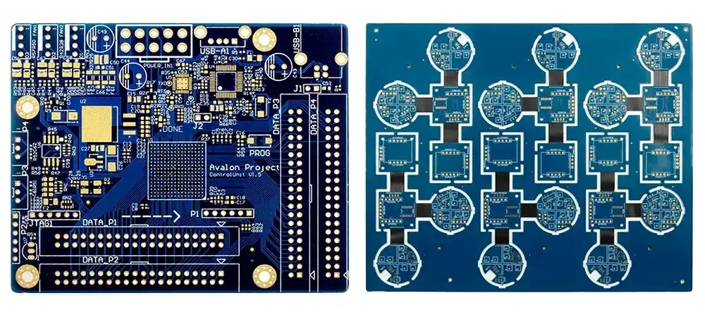
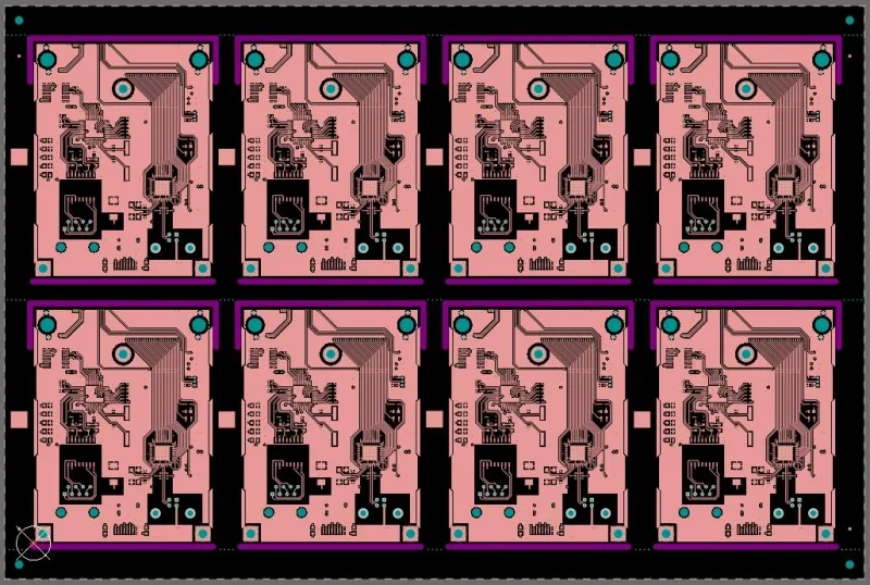
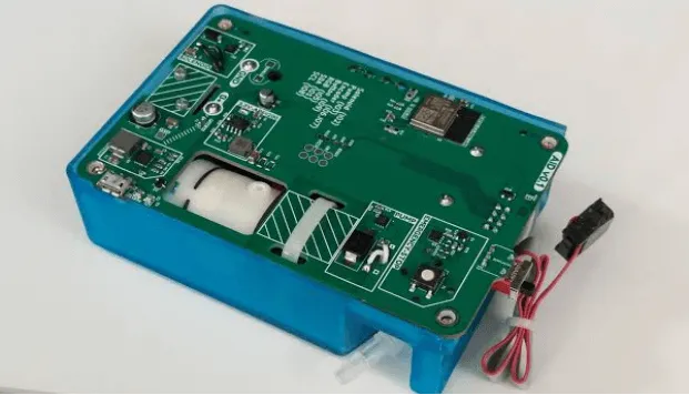
Standard PCB sizes refer to predefined dimensions and panel configurations commonly used across fabrication facilities to maximize material utilization and equipment compatibility. These sizes typically align with common panel formats that support efficient routing, etching, and depaneling processes in volume production. For instance, rectangular boards in multiples that fit standard panel dimensions reduce scrap and setup times, directly contributing to PCB cost optimization. Custom PCB fabrication involves tailoring board outlines, cutouts, and contours to specific mechanical requirements, often resulting in non-rectangular or irregular shapes.
The distinction matters because standard sizes benefit from shared tooling and process standardization, lowering per-unit costs for prototypes and production runs alike. Custom options shine in applications where mechanical integration demands precision, such as compact consumer electronics or aerospace modules. However, deviations from standards can increase non-recurring engineering (NRE) costs due to specialized fixturing and handling. Engineers must evaluate project scale and tolerances to determine the most suitable path, ensuring alignment with overall PCB design for manufacturing goals.
Why Form Factor Choices Impact PCB Costs
Form factor decisions influence every stage of the PCB lifecycle, from design validation to final assembly. Standard PCB sizes enable panelization strategies where multiple boards share a single substrate, optimizing material use and reducing handling overhead. This approach minimizes raw material waste and accelerates throughput, key factors in reducing PCB costs for mid-to-high volume orders. Custom shapes, while enabling tighter packaging, often require dedicated panels or v-scoring adjustments, potentially lowering panel efficiency to below 70% utilization in extreme cases.
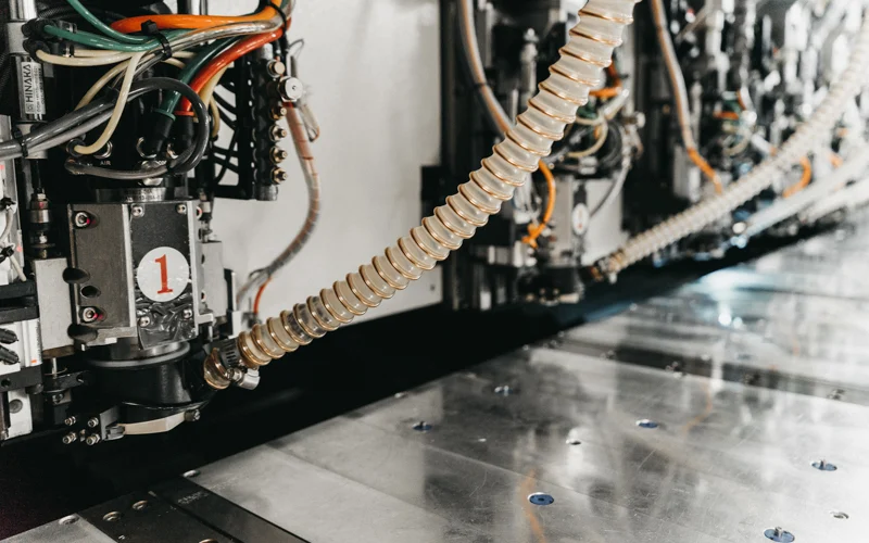
Cost implications extend beyond fabrication to testing and assembly phases. Standard formats facilitate automated optical inspection (AOI) and in-circuit testing (ICT) with universal fixtures, whereas custom contours may necessitate bespoke jigs, inflating setup expenses. Yield rates also play a role; irregular perimeters heighten risks of edge defects during lamination or plating, indirectly raising costs through rework. By quantifying these effects during the design phase, engineers can forecast total cost of ownership and pivot toward cost-effective alternatives without compromising performance.
Technical Principles Governing Form Factor Selections
The engineering principles behind form factor choices stem from material behavior, process physics, and equipment constraints. PCB substrates expand and contract during thermal cycles in lamination and reflow, with rectangular standards minimizing warpage gradients per IPC-A-600 guidelines for board acceptability. Custom designs with thin necks or large aspect ratios amplify stress concentrations, potentially leading to microcracks under mechanical stress. Engineers apply finite element analysis (FEA) to simulate these effects, ensuring compliance with performance specifications.
Panelization principles further dictate efficiency. Standard PCB sizes allow symmetric arrays that distribute fiducials evenly, aiding alignment in exposure and drilling steps. Custom fabrication disrupts this symmetry, requiring compensation in CAM software for routing paths and tabbing. Aspect ratios, defined as board length-to-thickness, must stay within recommended limits to prevent drill wander or via plating voids, principles outlined in generic design standards like IPC-2221B. These technical foundations underscore why standard options often yield superior dimensional stability and cost predictability.
Manufacturing tolerances add another layer. Standard sizes benefit from calibrated processes honed over high volumes, achieving tighter tolerances at lower cost. Custom profiles demand iterative prototyping to dial in depaneling methods like milling versus routing, each with unique burr and stress implications. By grounding decisions in these principles, designers mitigate risks and enhance PCB design for manufacturing compatibility.
Pros and Cons of Standard Versus Custom Form Factors
- Cost Structure
- Standard PCB Sizes: Lower NRE; economies from shared panels
- Custom PCB Fabrication: Higher tooling; per-unit savings in low volume
- Manufacturing Yield
- Standard PCB Sizes: High due to optimized processes
- Custom PCB Fabrication: Variable; depends on complexity
- Design Flexibility
- Standard PCB Sizes: Limited to rectangular norms
- Custom PCB Fabrication: Full contour control for enclosures
- Scalability
- Standard PCB Sizes: Excellent for volume production
- Custom PCB Fabrication: Better for prototypes or unique apps
- Risk Profile
- Standard PCB Sizes: Predictable defects and testing
- Custom PCB Fabrication: Elevated warpage, handling issues
Standard PCB sizes excel in scalability, where panel efficiency directly translates to reduced PCB costs through bulk material pricing and faster cycle times. Their uniformity simplifies supply chain logistics, from stackup verification to conformal coating application. Drawbacks include constraints on mechanical fit, sometimes requiring adapters that add assembly steps.
Custom PCB fabrication offers unmatched integration, allowing tabs, slots, or chamfers that eliminate secondary machining. This precision suits high-reliability sectors where every millimeter counts. However, the cons are pronounced in cost overruns from extended lead times and qualification testing. For electric engineers, a hybrid approach—starting with standards and iterating to custom only if essential—often balances these trade-offs effectively.
Best Practices for Cost-Effective PCB Form Factor Decisions
To achieve PCB cost optimization, begin with a design review that prioritizes standard PCB sizes unless mechanical imperatives dictate otherwise. Conduct a panelization study early, aiming for 80-90% utilization by arranging boards in even grids with adequate borders for routing. Incorporate design for manufacturing (DFM) rules, such as minimum web widths between boards and symmetric fiducial placement, to avoid common pitfalls.
For custom needs, simplify outlines by using straight lines and arcs over complex curves, reducing milling time by up to 30% in routing operations. Validate warpage potential through coupon testing aligned with IPC standards, adjusting copper balance if imbalances exceed thresholds. Collaborate with fabrication partners during the quoting phase to explore compromises, like modular standards with minor cutouts.
Leverage simulation tools for thermal and mechanical modeling before committing to prototypes. This proactive stance minimizes iterations, directly reducing PCB costs. Document tolerances explicitly, specifying edge finish and chamfer requirements to prevent misinterpretation. These practices ensure robust, economical designs across project scales.
Real-World Insights: When Custom Pays Off
In high-density interconnect (HDI) applications, custom PCB fabrication enables stacked vias and blind/buried configurations that standard rectangles cannot accommodate efficiently. Engineers report success by nesting irregular shapes within larger standard panels, recapturing some efficiency losses. For example, a compact IoT module benefited from contoured edges that integrated snap-fits, eliminating housing fasteners and assembly labor.
Conversely, consumer wearables sticking to standard sizes scaled production rapidly, achieving cost targets through automated lines. Troubleshooting tip: If custom warpage exceeds 0.75% bow/twist, revisit stackup symmetry or add stiffeners. These insights highlight context-driven choices, reinforcing PCB design for manufacturing as a holistic discipline.
Conclusion
Navigating standard versus custom PCB form factors demands a structured evaluation of cost, manufacturability, and application needs. Standard PCB sizes provide a reliable foundation for PCB cost optimization and volume efficiency, while custom fabrication unlocks innovation at a premium. By applying technical principles, DFM best practices, and strategic panelization, electric engineers can reduce PCB costs without sacrificing reliability. Prioritize simulations, standards compliance, and iterative reviews to future-proof designs. Ultimately, informed form factor selection transforms potential expenses into competitive advantages, streamlining the path from concept to production.
FAQs
Q1: What are common standard PCB sizes for PCB cost optimization?
A1: Standard PCB sizes typically include panel formats like 18 by 24 inches or Eurocard dimensions, optimized for high-volume fabrication. These allow efficient arraying, reducing material waste and setup costs. Engineers achieve PCB cost optimization by designing boards as multiples that maximize panel yield, often exceeding 85% utilization. Always verify compatibility with target processes to ensure seamless scaling.
Q2: When should you opt for custom PCB fabrication over standard sizes?
A2: Choose custom PCB fabrication when mechanical constraints, such as irregular enclosures or integrated features, outweigh cost premiums. It excels in low-volume prototypes or specialized applications needing precise contours. Balance this with DFM analysis to mitigate higher NRE and yield risks. Standard sizes suffice for most scalable projects focused on reducing PCB costs.
Q3: How does PCB design for manufacturing influence form factor choices?
A3: PCB design for manufacturing emphasizes panel efficiency, tolerance control, and process compatibility in form factor selection. Incorporate rules like even symmetry and fiducial placement to favor standards for cost savings. Custom designs require enhanced modeling to address warpage and routing challenges. This approach ensures reliable production while targeting PCB cost optimization.
Q4: What strategies help in reducing PCB costs with form factor options?
A4: Key strategies include starting with standard PCB sizes for panelization efficiency and only customizing essentials. Simulate warpage, optimize outlines, and quote multiple scenarios early. Hybrid panels blending standards with minor customs recapture savings. Consistent DFM adherence across teams minimizes iterations, directly lowering overall expenses.
References
IPC-A-600K — Acceptability of Printed Boards. IPC, 2020
IPC-2221B — Generic Standard on Printed Board Design. IPC, 2012
IPC-6012E — Qualification and Performance Specification for Rigid Printed Boards. IPC, 2015