Introduction
For electronic hobbyists, crafting a printed circuit board (PCB) at home is a rewarding challenge that offers hands-on learning and customization. While single and double-layer PCBs are common in DIY projects, creating multilayer boards with inner layers often seems out of reach due to complex manufacturing processes. However, with home PCB etching techniques, it is possible to experiment with inner layers for more advanced designs. This guide explores the process of making inner layers using DIY PCB production methods, focusing on practical steps and safe practices. Whether you are prototyping a complex circuit or learning advanced fabrication, understanding home etching for multilayer boards opens new possibilities. Let us dive into the essentials of this intricate yet achievable process for hobbyists.
What Are Inner Layers and Why Do They Matter
Inner layers in a PCB are the conductive copper planes sandwiched between insulating substrates in multilayer boards. Unlike the outer layers, which host most components and visible traces, inner layers provide additional routing space, power distribution, and ground planes. They are critical for high-density designs where space is limited, and signal integrity is paramount. For electronic hobbyists, inner layers enable more compact and efficient circuits without resorting to larger boards.
The relevance of inner layers lies in their ability to reduce electromagnetic interference and improve thermal management. By dedicating entire layers to ground or power, noise is minimized, and current distribution becomes more stable. For DIY PCB production, mastering inner layers means tackling professional-grade projects at home, pushing the boundaries of what hobbyists can achieve with limited tools.
Technical Principles of Inner Layers in PCB Etching
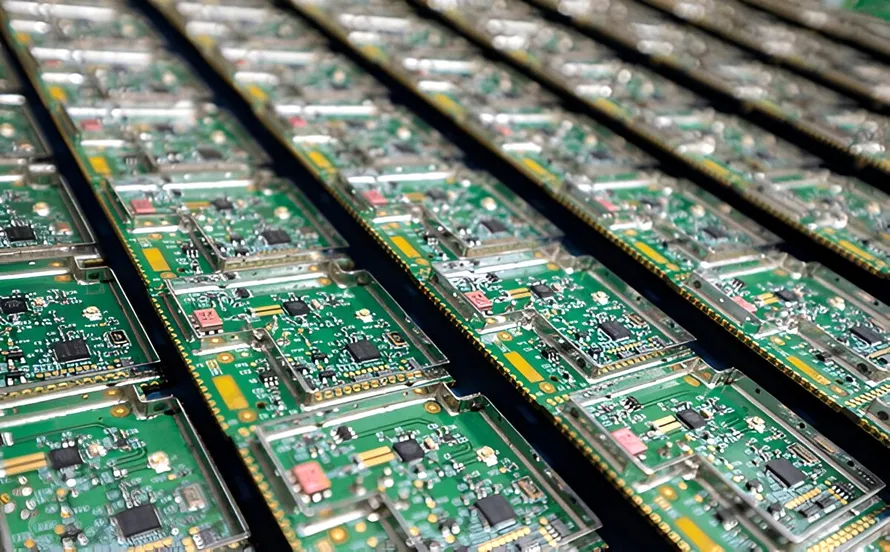
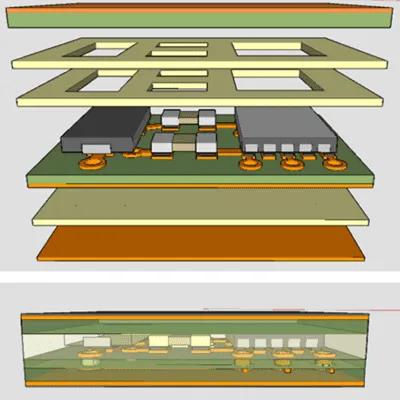
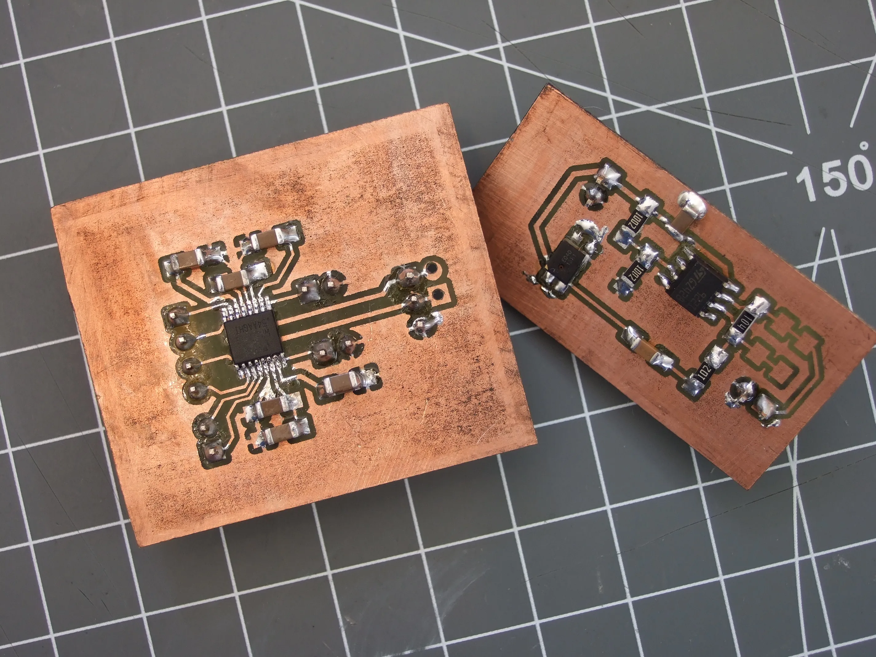
Creating inner layers at home starts with understanding the structure of multilayer boards. A typical four layer PCB consists of two outer layers and two inner layers, separated by insulating material like FR-4, a glass fiber and epoxy composite. Each copper layer is etched to form traces or planes before being laminated together under heat and pressure.
In professional settings, inner layers are etched using photolithography and automated processes to ensure precision. For home PCB etching, the principle remains the same: selectively remove copper from a clad board to form the desired pattern. The challenge lies in aligning multiple layers and bonding them without specialized equipment. Hobbyists must replicate this by carefully transferring designs onto copper, etching away unwanted material, and stacking layers with accuracy.
Etching involves a chemical reaction where an etchant, often ferric chloride or a vinegar-peroxide mix, dissolves exposed copper while a resist protects the intended traces. For inner layers, this process must be repeated for each layer before assembly. Alignment is critical, as misregistration can lead to short circuits or broken connections. Additionally, vias, which connect layers, require precise drilling and plating, a step that is tricky in DIY setups.
Step-by-Step Guide to Making Inner Layers with Home Etching
Creating inner layers for the multilayer PCB at home demands patience, precision, and safety. Below is a detailed guide tailored for electronic hobbyists venturing into DIY PCB production with home PCB etching methods.
Step 1: Design and Planning
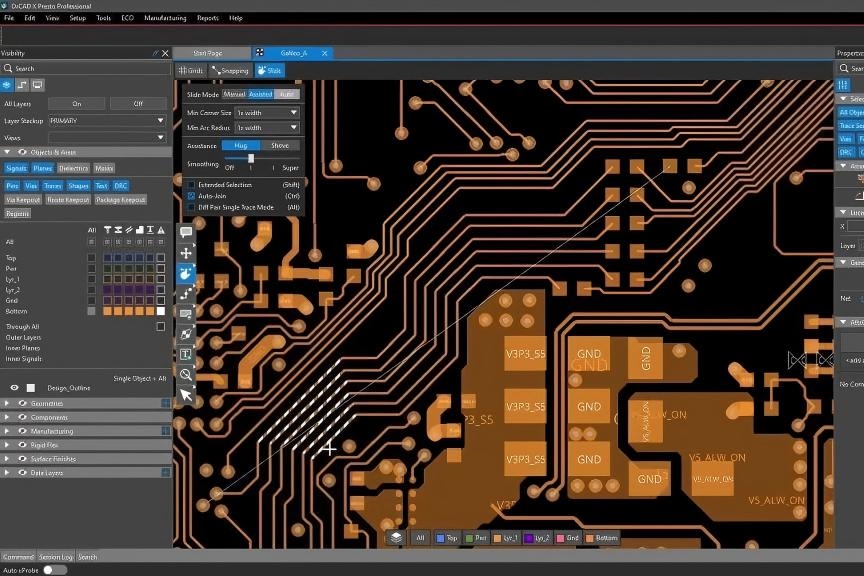
Begin by designing your multilayer PCB using suitable software that supports layer stacking. Ensure each inner layer is clearly defined with traces, planes, and alignment markers. Print the designs for each layer on transparent film or paper, ensuring they are scaled correctly. Include registration marks on all layers to aid alignment during assembly. Double-check the layout for errors, as mistakes in inner layers are nearly impossible to fix post-lamination.
Step 2: Prepare Copper-Clad Boards
Select thin copper-clad boards, ideally 0.8 mm or less, for inner layers to keep the final stack manageable. Clean the boards thoroughly with steel wool or abrasive pads to remove oxidation and ensure a smooth surface. Handle them with gloves to avoid fingerprints, which can interfere with resist application. Cut the boards to match the dimensions of your design, allowing a small margin for trimming later.
Step 3: Transfer Designs to Inner Layers
Apply a photoresist film or use a toner transfer method to place your design onto the copper. For photoresist, expose the board to UV light through the printed transparency, then develop it to reveal the pattern. For toner transfer, print the design with a laser printer and iron it onto the copper surface. Ensure the transfer is clear and free of smudges, as this resist will protect the copper during etching. Repeat this for each inner layer board.
Step 4: Etch the Inner Layers
Prepare your etchant solution in a well-ventilated area, following safety guidelines. Common etchants for home use include ferric chloride or a mixture of hydrogen peroxide and vinegar with salt. Submerge the boards in the solution, agitating gently to ensure even etching. Monitor the process closely to avoid over-etching, which can damage fine traces. Once the exposed copper is removed, rinse the boards in water and remove the resist using acetone or a suitable solvent.
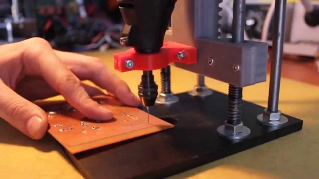
Step 5: Inspect and Drill Vias
After etching, inspect each inner layer under bright light for defects like incomplete traces or shorts. Use a multimeter to test continuity if needed. Mark via locations based on your design and drill holes using a precision drill bit, typically 0.8 to 1.2 mm in diameter. Ensure the holes align across all layers by using a drilling template or registration marks. Clean any burrs from drilling to prevent issues during stacking.
Step 6: Align and Laminate Layers
Stack the inner layers with insulating material, such as prepreg or thin FR-4 sheets, between them. Use alignment pins or registration holes to ensure precise positioning. Apply even pressure and heat using a laminating press or a household iron set to a low temperature. Be cautious to avoid shifting layers during this step. Allow the stack to cool under pressure to ensure a strong bond.
Step 7: Add Outer Layers and Finalize
Once the inner layers are laminated, add the outer copper-clad boards with their respective designs transferred and etched. Drill through-holes for vias that connect all layers. For conductivity through vias, insert rivets or use conductive epoxy as a substitute for professional plating. Test the board for continuity across layers to confirm connections are intact.
Step 8: Safety and Cleanup
Always prioritize safety during home PCB etching. Wear gloves, goggles, and protective clothing when handling chemicals. Work in a ventilated space to avoid inhaling fumes. Dispose of used etchant responsibly, following local regulations for chemical waste. Clean all tools and workspace to prevent contamination or accidents in future projects.
Challenges and Troubleshooting for DIY Inner Layers
Creating inner layers at home is not without hurdles. Misalignment during lamination is a common issue, leading to non-functional boards. To mitigate this, use multiple registration marks and double-check alignment before applying heat. Another challenge is achieving reliable via connections without professional plating. Conductive paints or small rivets can work, but they require careful application to avoid shorts.
Etching inconsistencies can also arise due to uneven resist application or etchant strength. Test your process on a scrap board before working on the actual layers. If traces are too thin or break during etching, adjust the exposure time or etchant concentration. Finally, lamination may result in air bubbles or delamination if pressure and heat are uneven. Applying gradual, consistent pressure helps minimize these defects.
Best Practices for Home PCB Etching of Inner Layers
To achieve success in DIY PCB production with inner layers, follow these best practices. First, always start with a small, simple multilayer design to practice the process before scaling up to complex boards. Second, maintain a clean workspace to avoid dust or debris interfering with resist or lamination. Third, document each step, including etchant mix ratios and timing, to replicate successful results.
Invest in basic tools like a precision drill press and magnifying glass to improve accuracy. Use high-quality materials, even for home projects, as poor substrates or copper can lead to failures. Finally, adhere to safety protocols without exception, as chemical handling poses significant risks if not managed properly. By refining these skills, hobbyists can push their projects closer to professional standards.
Conclusion
Crafting inner layers for multilayer PCBs using home PCB etching methods is a challenging yet achievable goal for electronic hobbyists. By following a structured approach, from design and etching to alignment and lamination, it is possible to create functional multilayer boards in a DIY setting. While the process demands precision and patience, the ability to prototype advanced circuits at home is a valuable skill. With practice and adherence to best practices, hobbyists can overcome the limitations of basic setups and explore the full potential of DIY PCB production. This guide serves as a foundation to start experimenting with inner layers, paving the way for more innovative projects.
FAQs
Q1: What materials are best for home PCB etching of inner layers?
A1: For home PCB etching, use thin copper-clad FR-4 boards, ideally 0.8 mm or less, for inner layers. Photoresist film or toner transfer paper works well for design application. Common etchants like ferric chloride or a vinegar-peroxide mix are effective and accessible. Ensure insulating prepreg or thin epoxy sheets for lamination to maintain structural integrity between layers.
Q2: How can I ensure alignment when making inner layers at home?
A2: Alignment in DIY PCB production is critical. Include registration marks on all layer designs and drill alignment holes before etching. Use pins or a jig to hold layers in place during stacking. Double-check positioning under bright light before lamination to avoid misregistration, which can ruin the board's functionality.
Q3: What are the safety risks of home PCB etching for inner layers?
A3: Home PCB etching involves chemicals like ferric chloride, which can cause skin irritation or respiratory issues if inhaled. Always work in a ventilated area, wear gloves, goggles, and protective clothing. Dispose of used etchants per local guidelines to avoid environmental harm. Keep tools and chemicals away from children or pets.
Q4: Can I create vias in inner layers during DIY PCB production?
A4: Yes, vias are possible in DIY PCB production by drilling precise holes after etching each layer. Align holes using registration marks. For conductivity, use small rivets or conductive epoxy, as professional plating is not feasible at home. Test continuity with a multimeter to ensure reliable connections across layers.
References
IPC-6012E — Qualification and Performance Specification for Rigid Printed Boards. IPC, 2020.
IPC-A-600K — Acceptability of Printed Boards. IPC, 2020.
IPC-2221B — Generic Standard on Printed Board Design. IPC, 2012.